PSMN030-150B,118 NXP Semiconductors, PSMN030-150B,118 Datasheet - Page 2
PSMN030-150B,118
Manufacturer Part Number
PSMN030-150B,118
Description
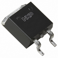
MOSFET N-CH 150V 55.5A SOT404
Manufacturer
NXP Semiconductors
Series
TrenchMOS™r
Datasheet
1.PSMN030-150B118.pdf
(12 pages)
Specifications of PSMN030-150B,118
Package / Case
D²Pak, TO-263 (2 leads + tab)
Mounting Type
Surface Mount
Power - Max
250W
Fet Type
MOSFET N-Channel, Metal Oxide
Gate Charge (qg) @ Vgs
98nC @ 10V
Vgs(th) (max) @ Id
4V @ 1mA
Current - Continuous Drain (id) @ 25° C
55.5A
Drain To Source Voltage (vdss)
150V
Fet Feature
Standard
Rds On (max) @ Id, Vgs
30 mOhm @ 25A, 10V
Minimum Operating Temperature
- 55 C
Configuration
Single
Transistor Polarity
N-Channel
Resistance Drain-source Rds (on)
0.03 Ohm @ 10 V
Drain-source Breakdown Voltage
150 V
Gate-source Breakdown Voltage
+/- 20 V
Continuous Drain Current
55.5 A
Power Dissipation
250000 mW
Maximum Operating Temperature
+ 175 C
Mounting Style
SMD/SMT
Lead Free Status / RoHS Status
Lead free / RoHS Compliant
Lead Free Status / RoHS Status
Lead free / RoHS Compliant, Lead free / RoHS Compliant
Other names
934056598118::PSMN030-150B /T3::PSMN030-150B /T3


NXP Semiconductors
2. Pinning information
Table 2.
[1]
3. Ordering information
Table 3.
4. Limiting values
Table 4.
In accordance with the Absolute Maximum Rating System (IEC 60134).
PSMN030-150B
Product data sheet
Pin
1
2
3
mb
Type number
PSMN030-150B
Symbol
V
V
V
I
I
P
T
T
Source-drain diode
I
I
Avalanche ruggedness
E
I
D
DM
S
SM
AS
stg
j
DS
DGR
GS
tot
DS(AL)S
It not possible to make a connection to pin 2.
Symbol Description
G
D
S
D
Pinning information
Ordering information
Limiting values
Parameter
drain-source voltage
drain-gate voltage
gate-source voltage
drain current
peak drain current
total power dissipation
storage temperature
junction temperature
source current
peak source current
non-repetitive drain-source
avalanche energy
non-repetitive avalanche current
gate
drain
source
mounting base; connected to drain
D2PAK
Package
Name
[1]
Description
plastic single-ended surface-mounted package (D2PAK); 3 leads
(one lead cropped)
All information provided in this document is subject to legal disclaimers.
Rev. 02 — 13 December 2010
Conditions
T
T
T
T
pulsed; T
T
T
pulsed; T
V
V
t
V
R
p
j
j
mb
mb
mb
mb
GS
sup
sup
GS
Simplified outline
= 100 µs
≥ 25 °C; T
≤ 175 °C; T
N-channel TrenchMOS SiliconMAX standard level FET
= 25 °C
= 100 °C
= 25 °C
= 25 °C
= 10 V; T
= 50 Ω; unclamped
≤ 50 V; unclamped; R
≤ 50 V; V
SOT404 (D2PAK)
mb
mb
= 25 °C
= 25 °C
j
≤ 175 °C
j
j(init)
GS
≥ 25 °C; R
1
= 10 V; T
mb
2
= 25 °C; I
3
GS
j(init)
GS
D
= 20 kΩ
= 35 A;
= 50 Ω;
= 25 °C;
PSMN030-150B
Graphic symbol
Min
-
-
-20
-
-
-
-
-55
-55
-
-
-
-
mbb076
G
© NXP B.V. 2010. All rights reserved.
175
175
Version
SOT404
Max
150
150
20
55.5
39
222
250
55.5
222
300
35
D
S
Unit
V
V
V
A
A
A
W
°C
°C
A
A
mJ
A
2 of 12
Related parts for PSMN030-150B,118
Image
Part Number
Description
Manufacturer
Datasheet
Request
R

Part Number:
Description:
MOSFET,N CH,60V,29A,LFPAK
Manufacturer:
NXP Semiconductors
Datasheet:

Part Number:
Description:
SiliconMAX standard level N-channel enhancement mode Field-Effect Transistor (FET) in a plastic package using TrenchMOS technology
Manufacturer:
NXP Semiconductors
Datasheet:

Part Number:
Description:
SiliconMAX standard level N-channel enhancement mode Field-Effect Transistor (FET) in a plastic package using TrenchMOS technology
Manufacturer:
NXP Semiconductors
Datasheet:

Part Number:
Description:
MOSFET N-CH 150V 55.5A SOT78
Manufacturer:
NXP Semiconductors
Datasheet:

Part Number:
Description:
MOSFET TAPE13 MOSFET
Manufacturer:
NXP Semiconductors
Datasheet:

Part Number:
Description:
MOSFET N-CH LFPAK
Manufacturer:
NXP Semiconductors
Datasheet:

Part Number:
Description:
N-channel TrenchMOS SiliconMAX standard level FET
Manufacturer:
NXP [NXP Semiconductors]
Datasheet:
Part Number:
Description:
N-channel LFPAK 60 V 24.7 m? standard level MOSFET
Manufacturer:
PHILIPS [NXP Semiconductors]
Datasheet:
Part Number:
Description:
NXP Semiconductors designed the LPC2420/2460 microcontroller around a 16-bit/32-bitARM7TDMI-S CPU core with real-time debug interfaces that include both JTAG andembedded trace
Manufacturer:
NXP Semiconductors
Datasheet:

Part Number:
Description:
NXP Semiconductors designed the LPC2458 microcontroller around a 16-bit/32-bitARM7TDMI-S CPU core with real-time debug interfaces that include both JTAG andembedded trace
Manufacturer:
NXP Semiconductors
Datasheet:
Part Number:
Description:
NXP Semiconductors designed the LPC2468 microcontroller around a 16-bit/32-bitARM7TDMI-S CPU core with real-time debug interfaces that include both JTAG andembedded trace
Manufacturer:
NXP Semiconductors
Datasheet:
Part Number:
Description:
NXP Semiconductors designed the LPC2470 microcontroller, powered by theARM7TDMI-S core, to be a highly integrated microcontroller for a wide range ofapplications that require advanced communications and high quality graphic displays
Manufacturer:
NXP Semiconductors
Datasheet:
Part Number:
Description:
NXP Semiconductors designed the LPC2478 microcontroller, powered by theARM7TDMI-S core, to be a highly integrated microcontroller for a wide range ofapplications that require advanced communications and high quality graphic displays
Manufacturer:
NXP Semiconductors
Datasheet:
Part Number:
Description:
The Philips Semiconductors XA (eXtended Architecture) family of 16-bit single-chip microcontrollers is powerful enough to easily handle the requirements of high performance embedded applications, yet inexpensive enough to compete in the market for hi
Manufacturer:
NXP Semiconductors
Datasheet: