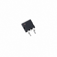
STB80NF55-08T4 STMicroelectronics, STB80NF55-08T4 Datasheet

STB80NF55-08T4
Specifications of STB80NF55-08T4
Available stocks
Related parts for STB80NF55-08T4
STB80NF55-08T4 Summary of contents
Page 1
... Total Dissipation at T tot Derating Factor AS (1) E Single Pulse Avalanche Energy T Storage Temperature stg T Max. Operating Junction Temperature j ( Current limited by package ( Pulse width limited by safe operating area. March 2002 . STB80NF55-08 STB80NF55-08-1 - 80A D STripFET™ II POWER MOSFET R I DS(on TO-263 therefore a INTERNAL SCHEMATIC DIAGRAM = 25° ...
Page 2
... STB80NF55-08/-1 STP80NF55-08 THERMAL DATA Rthj-case Thermal Resistance Junction-case Rthj-amb Thermal Resistance Junction-ambient T Maximum Lead Temperature For Soldering Purpose l ELECTRICAL CHARACTERISTICS (T OFF Symbol Parameter Drain-source V (BR)DSS Breakdown Voltage Zero Gate Voltage I DSS Drain Current (V GS Gate-body Leakage I GSS Current ( (*) ON Symbol Parameter V Gate Threshold Voltage ...
Page 3
... Source-drain Current (pulsed) SD (*) V Forward On Voltage t Reverse Recovery Time rr Q Reverse Recovery Charge rr Reverse Recovery Current I RRM (*) Pulsed: Pulse duration = 300 µs, duty cycle 1 Pulse width limited by safe operating area. Safe Operating Area STB80NF55-08/-1 STP80NF55-08 Test Conditions 4 (Resistive Load, Figure 44V ...
Page 4
... STB80NF55-08/-1 STP80NF55-08 Output Characteristics Transconductance Gate Charge vs Gate-source Voltage 4/11 Transfer Characteristics Static Drain-source On Resistance Capacitance Variations ...
Page 5
... Normalized Gate Threshold Voltage vs Temperature Source-drain Diode Forward Characteristics . . STB80NF55-08/-1 STP80NF55-08 Normalized on Resistance vs Temperature Normalized Breakdown Voltage vs Temperature 5/11 ...
Page 6
... STB80NF55-08/-1 STP80NF55-08 Fig. 1: Unclamped Inductive Load Test Circuit Fig. 1: Unclamped Inductive Load Test Circuit Fig. 3: Switching Times Test Circuits For Resistive Load Fig. 5: Test Circuit For Inductive Load Switching And Diode Recovery Times 6/11 Fig. 2: Unclamped Inductive Waveform Fig. 4: Gate Charge test Circuit ...
Page 7
... STB80NF55-08/-1 STP80NF55-08 inch. TYP. TYP. 0.181 0.106 0.009 0.037 0.067 0.024 0.054 0.368 0.315 0.409 0.334 0.208 0.624 0.055 0.069 0.126 0.016 0° ...
Page 8
... STB80NF55-08/-1 STP80NF55-08 TO-262 (I DIM. MIN. A 4.4 A1 2.49 B 0.7 B2 1.14 C 0.45 C2 1.23 D 8. 13.1 L1 3.48 L2 1.27 L2 8/11 2 PAK) MECHANICAL DATA mm TYP. MAX. MIN. 4.6 0.173 2.69 0.098 0.93 0.027 1.7 0.044 0.6 0.017 1.36 0.048 9.35 0.352 2.7 0.094 10.4 0.393 13 ...
Page 9
... F1 1.14 F2 1.14 G 4.95 G1 2 13.0 L5 2.65 L6 15.25 L7 6.2 L9 3.5 DIA. 3.75 Dia STB80NF55-08/-1 STP80NF55-08 mm MAX. MIN. 4.60 0.173 1.32 0.048 2.72 0.094 1.27 0.70 0.019 0.88 0.024 1.70 0.044 1.70 0.044 5.15 0.194 2.7 0.094 10.40 0.393 16.4 14.0 ...
Page 10
... STB80NF55-08/-1 STP80NF55- PAK FOOTPRINT TAPE AND REEL SHIPMENT (suffix ”T4”)* TAPE MECHANICAL DATA mm DIM. MIN. MAX. MIN. A0 10.5 10.7 0.413 B0 15.7 15.9 0.618 D 1.5 1.6 0.059 D1 1.59 1.61 0.062 E 1.65 1.85 0.065 F 11.4 11.6 0.449 K0 4.8 5.0 0.189 P0 3.9 4.1 ...
Page 11
... Australia - Brazil - Canada - China - Finland - France - Germany - Hong Kong - India - Israel - Italy - Japan - Malaysia - Malta - Morocco - Singapore - Spain - Sweden - Switzerland - United Kingdom - United States. The ST logo is registered trademark of STMicroelectronics 2002 STMicroelectronics - All Rights Reserved All other names are the property of their respective owners. STMicroelectronics GROUP OF COMPANIES http://www.st.com STB80NF55-08/-1 STP80NF55-08 11/11 ...
Page 12
This datasheet has been download from: www.datasheetcatalog.com Datasheets for electronics components. ...


