IRFS4115-7PPBF International Rectifier, IRFS4115-7PPBF Datasheet - Page 2
IRFS4115-7PPBF
Manufacturer Part Number
IRFS4115-7PPBF
Description
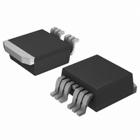
MOSFET N-CH 150V 105A D2PAK-7
Manufacturer
International Rectifier
Series
HEXFET®r
Datasheet
1.IRFS4115TRL7PP.pdf
(9 pages)
Specifications of IRFS4115-7PPBF
Fet Type
MOSFET N-Channel, Metal Oxide
Fet Feature
Standard
Rds On (max) @ Id, Vgs
11.8 mOhm @ 63A, 10V
Drain To Source Voltage (vdss)
150V
Current - Continuous Drain (id) @ 25° C
105A
Vgs(th) (max) @ Id
5V @ 250µA
Gate Charge (qg) @ Vgs
110nC @ 10V
Input Capacitance (ciss) @ Vds
5320pF @ 50V
Power - Max
380W
Mounting Type
Surface Mount
Package / Case
D²Pak, TO-263 (6 leads + tab)
Transistor Polarity
N-Channel
Drain-source Breakdown Voltage
150 V
Gate-source Breakdown Voltage
20 V
Continuous Drain Current
105 A
Power Dissipation
380 W
Mounting Style
SMD/SMT
Gate Charge Qg
73 nC
Lead Free Status / RoHS Status
Lead free / RoHS Compliant
Available stocks
Company
Part Number
Manufacturer
Quantity
Price

Part Number:
IRFS4115-7PPBF
Manufacturer:
IR
Quantity:
20 000


Notes:
‚
ƒ
„
Static @ T
V
ΔV
R
V
I
I
R
Dynamic @ T
gfs
Q
Q
Q
Q
t
t
t
t
C
C
C
C
C
Diode Characteristics
I
I
V
t
Q
I
t
DSS
GSS
d(on)
r
d(off)
f
S
SM
rr
RRM
on
(BR)DSS
GS(th)
SD
DS(on)
G(int)
iss
oss
rss
oss
oss
g
gs
gd
sync
rr
Repetitive rating; pulse width limited by max. junction
Limited by T
Pulse width ≤ 400μs; duty cycle ≤ 2%.
2
temperature.
use above this value.
I
R
Symbol
Symbol
Symbol
SD
(BR)DSS
G
eff. (ER) Effective Output Capacitance (Energy Related)h –––
eff. (TR) Effective Output Capacitance (Time Related)g
≤ 63A, di/dt ≤ 2510A/μs, V
= 25Ω, I
/ΔT
J
AS
Jmax
J
Drain-to-Source Breakdown Voltage
Breakdown Voltage Temp. Coefficient
Static Drain-to-Source On-Resistance
Gate Threshold Voltage
Drain-to-Source Leakage Current
Gate-to-Source Forward Leakage
Gate-to-Source Reverse Leakage
Internal Gate Resistance
Forward Transconductance
Total Gate Charge
Gate-to-Source Charge
Gate-to-Drain ("Miller") Charge
Total Gate Charge Sync. (Q
Turn-On Delay Time
Rise Time
Turn-Off Delay Time
Fall Time
Input Capacitance
Output Capacitance
Reverse Transfer Capacitance
Continuous Source Current
(Body Diode)
Pulsed Source Current
(Body Diode) c
Diode Forward Voltage
Reverse Recovery Time
Reverse Recovery Charge
Reverse Recovery Current
Forward Turn-On Time
= 63A, V
= 25°C (unless otherwise specified)
, starting T
J
= 25°C (unless otherwise specified)
Parameter
GS
=10V. Part not recommended for
J
= 25°C, L = 0.115mH
DD
≤ V
Parameter
Parameter
(BR)DSS
, T
J
g
≤ 175°C.
- Q
gd
)
Intrinsic turn-on time is negligible (turn-on is dominated by LS+LD)
…
†
‡
ˆ
‰
Min. Typ. Max. Units
Min. Typ. Max. Units
Min. Typ. Max. Units
–––
–––
–––
–––
–––
–––
150
–––
–––
–––
–––
–––
–––
–––
–––
–––
–––
–––
–––
–––
–––
–––
–––
–––
–––
–––
–––
–––
3.0
93
C
When mounted on 1" square PCB (FR-4 or G-10 Material). For recom
R
C
as C
C
mended footprint and soldering techniques refer to application note #AN-994.
oss
θ
oss
θJC
oss
is measured at T
eff. (TR) is a fixed capacitance that gives the same charging time
oss
eff. (ER) is a fixed capacitance that gives the same energy as
while V
5320
0.18
110
271
–––
–––
–––
–––
–––
–––
–––
490
450
520
–––
–––
–––
385
10.
2.1
6.0
73
28
28
45
18
50
37
23
82
99
while V
DS
-100
11.8
–––
–––
250
100
–––
–––
110
–––
–––
–––
–––
–––
–––
–––
–––
–––
–––
–––
–––
104
420
–––
–––
–––
–––
–––
5.0
1.3
20
is rising from 0 to 80% V
DS
is rising from 0 to 80% V
J
approximately 90°C.
V/°C
mΩ
nA
nC
nC
μA
pF
ns
ns
V
V
Ω
S
A
V
A
V
Reference to 25°C, I
V
V
V
V
V
V
V
I
V
V
I
V
I
R
V
V
V
ƒ = 1.0MHz
V
V
MOSFET symbol
showing the
integral reverse
p-n junction diode.
T
T
T
T
T
T
D
D
D
J
J
J
J
J
J
GS
GS
DS
DS
DS
GS
GS
DS
DS
GS
DD
GS
GS
DS
GS
GS
G
= 63A
= 63A, V
= 63A
= 25°C, I
= 25°C
= 125°C
= 25°C
= 125°C
= 25°C
= 2.1Ω
= 0V, I
= 10V, I
= V
= 150V, V
= 150V, V
= 20V
= -20V
= 50V, I
= 75V
= 10V f
= 98V
= 10V f
= 0V
= 50V
= 0V, V
= 0V, V
GS
, I
DSS
D
DS
D
S
DS
DS
D
D
= 250μA
DSS
.
= 63A, V
= 250μA
= 63A f
= 62A
=0V, V
GS
GS
= 0V to 120V h
= 0V to 120V g
Conditions
Conditions
Conditions
.
= 0V
= 0V, T
V
I
di/dt = 100A/μs f
F
R
= 63A
D
GS
= 130V,
GS
= 3.5mAc
= 10V
J
= 0V f
= 125°C
www.irf.com
G
D
S
Related parts for IRFS4115-7PPBF
Image
Part Number
Description
Manufacturer
Datasheet
Request
R

Part Number:
Description:
SCHOTTKY RECTIFIER
Manufacturer:
International Rectifier Corp.
Datasheet:
Part Number:
Description:
SCHOTTKY RECTIFIER
Manufacturer:
International Rectifier Corp.
Datasheet:
Part Number:
Description:
SCHOTTKY RECTIFIER
Manufacturer:
International Rectifier Corp.
Datasheet:
Part Number:
Description:
SCHOTTKY RECTIFIER
Manufacturer:
International Rectifier Corp.
Datasheet:
Part Number:
Description:
SCHOTTKY RECTIFIER
Manufacturer:
International Rectifier Corp.
Datasheet:
Part Number:
Description:
SCHOTTKY RECTIFIER
Manufacturer:
International Rectifier Corp.
Datasheet:
Part Number:
Description:
SCHOTTKY RECTIFIER
Manufacturer:
International Rectifier Corp.
Datasheet:
Part Number:
Description:
SCHOTTKY RECTIFIER
Manufacturer:
International Rectifier Corp.
Datasheet:
Part Number:
Description:
SCHOTTKY RECTIFIER
Manufacturer:
International Rectifier Corp.
Datasheet:
Part Number:
Description:
SCHOTTKY RECTIFIER
Manufacturer:
International Rectifier Corp.
Datasheet:
Part Number:
Description:
SCHOTTKY RECTIFIER
Manufacturer:
International Rectifier Corp.
Datasheet:
Part Number:
Description:
SCHOTTKY RECTIFIER
Manufacturer:
International Rectifier Corp.
Datasheet:
Part Number:
Description:
SCHOTTKY RECTIFIER
Manufacturer:
International Rectifier Corp.
Datasheet:
Part Number:
Description:
SCHOTTKY RECTIFIER
Manufacturer:
International Rectifier Corp.
Datasheet:
Part Number:
Description:
SCHOTTKY RECTIFIER
Manufacturer:
International Rectifier Corp.
Datasheet: