IPW90R1K0C3 Infineon Technologies, IPW90R1K0C3 Datasheet - Page 2
IPW90R1K0C3
Manufacturer Part Number
IPW90R1K0C3
Description
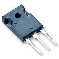
MOSFET N-CH 900V 5.7A TO-247
Manufacturer
Infineon Technologies
Series
CoolMOS™r
Specifications of IPW90R1K0C3
Fet Type
MOSFET N-Channel, Metal Oxide
Fet Feature
Standard
Rds On (max) @ Id, Vgs
1 Ohm @ 3.3A, 10V
Drain To Source Voltage (vdss)
900V
Current - Continuous Drain (id) @ 25° C
5.7A
Vgs(th) (max) @ Id
3.5V @ 370µA
Gate Charge (qg) @ Vgs
34nC @ 10V
Input Capacitance (ciss) @ Vds
850pF @ 100V
Power - Max
89W
Mounting Type
Through Hole
Package / Case
TO-247-3 (Straight Leads)
Transistor Polarity
N Channel
Continuous Drain Current Id
5.7A
Drain Source Voltage Vds
900V
On Resistance Rds(on)
1ohm
Rds(on) Test Voltage Vgs
10V
Voltage Vgs Max
20V
Operating Temperature Range
-55°C To
Threshold Voltage Vgs Typ
3V
Rohs Compliant
Yes
Configuration
Single
Resistance Drain-source Rds (on)
1 Ohms
Drain-source Breakdown Voltage
900 V
Gate-source Breakdown Voltage
+/- 20 V
Continuous Drain Current
5.7 A
Power Dissipation
89 W
Maximum Operating Temperature
+ 150 C
Mounting Style
Through Hole
Minimum Operating Temperature
- 55 C
Lead Free Status / RoHS Status
Lead free / RoHS Compliant
Lead Free Status / RoHS Status
Lead free / RoHS Compliant, Lead free / RoHS Compliant
Other names
SP000413752
Available stocks
Company
Part Number
Manufacturer
Quantity
Price
Company:

Part Number:
IPW90R1K0C3
Manufacturer:
INFINEON
Quantity:
12 500
Part Number:
IPW90R1K0C3
Manufacturer:
INFINEON/英飞凌
Quantity:
20 000


Please note the new package dimensions arccording to PCN 2009-134-A
Rev. 1.0
Maximum ratings, at T
Parameter
Continuous diode forward current
Diode pulse current
Reverse diode dv /dt
Parameter
Thermal characteristics
Thermal resistance, junction - case
Thermal resistance, junction -
ambient
Soldering temperature,
wavesoldering only allowed at leads
Electrical characteristics, at T
Static characteristics
Drain-source breakdown voltage
Gate threshold voltage
Zero gate voltage drain current
Gate-source leakage current
Drain-source on-state resistance
Gate resistance
2)
4)
J
=25 °C, unless otherwise specified
J
=25 °C, unless otherwise specified
Symbol Conditions
I
I
dv /dt
Symbol Conditions
R
R
T
V
V
I
I
R
R
S
S,pulse
DSS
GSS
sold
(BR)DSS
GS(th)
thJC
thJA
DS(on)
G
T
leaded
1.6 mm (0.063 in.)
from case for 10 s
V
V
V
T
V
T
V
V
T
V
T
f =1 MHz, open drain
page 2
C
j
j
j
j
GS
DS
DS
DS
GS
GS
GS
=25 °C
=150 °C
=25 °C
=150 °C
=25 °C
=V
=900 V, V
=900 V, V
=0 V, I
=20 V, V
=10 V, I
=10 V, I
GS
, I
D
D
=250 µA
D
D
=0.37 mA
DS
=3.3 A,
=3.3 A,
GS
GS
=0 V
=0 V,
=0 V,
min.
900
2.5
-
-
-
-
-
-
-
-
-
Values
Value
0.78
typ.
3.3
2.1
1.3
13
10
4
3
-
-
-
-
-
-
IPW90R1K0C3
max.
100
260
1.4
3.5
62
1
1
-
-
-
-
Unit
A
V/ns
Unit
K/W
°C
V
nA
µA
2008-07-29
Related parts for IPW90R1K0C3
Image
Part Number
Description
Manufacturer
Datasheet
Request
R

Part Number:
Description:
Manufacturer:
Infineon Technologies AG
Datasheet:
Part Number:
Description:
Manufacturer:
Infineon Technologies AG
Datasheet:
Part Number:
Description:
Manufacturer:
Infineon Technologies AG
Datasheet:
Part Number:
Description:
Manufacturer:
Infineon Technologies AG
Datasheet:
Part Number:
Description:
Manufacturer:
Infineon Technologies AG
Datasheet:
Part Number:
Description:
Manufacturer:
Infineon Technologies AG
Datasheet:
Part Number:
Description:
Manufacturer:
Infineon Technologies AG
Datasheet:
Part Number:
Description:
16-bit microcontroller with 2x2 KByte RAM
Manufacturer:
Infineon Technologies AG
Datasheet:
Part Number:
Description:
NPN silicon RF transistor
Manufacturer:
Infineon Technologies AG
Datasheet:
Part Number:
Description:
NPN silicon RF transistor
Manufacturer:
Infineon Technologies AG
Datasheet:
Part Number:
Description:
NPN silicon RF transistor
Manufacturer:
Infineon Technologies AG
Datasheet:
Part Number:
Description:
NPN silicon RF transistor
Manufacturer:
Infineon Technologies AG
Datasheet:
Part Number:
Description:
Si-MMIC-amplifier in SIEGET 25-technologie
Manufacturer:
Infineon Technologies AG
Datasheet:
Part Number:
Description:
IGBT Power Module
Manufacturer:
Infineon Technologies AG
Datasheet:
Part Number:
Description:
IC for switching-mode power supplies
Manufacturer:
Infineon Technologies AG
Datasheet: