IRF630S Vishay, IRF630S Datasheet - Page 3
IRF630S
Manufacturer Part Number
IRF630S
Description
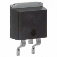
MOSFET N-CH 200V 9A D2PAK
Manufacturer
Vishay
Specifications of IRF630S
Fet Type
MOSFET N-Channel, Metal Oxide
Fet Feature
Standard
Rds On (max) @ Id, Vgs
400 mOhm @ 5.4A, 10V
Drain To Source Voltage (vdss)
200V
Current - Continuous Drain (id) @ 25° C
9A
Vgs(th) (max) @ Id
4V @ 250µA
Gate Charge (qg) @ Vgs
43nC @ 10V
Input Capacitance (ciss) @ Vds
800pF @ 25V
Power - Max
3W
Mounting Type
Surface Mount
Package / Case
D²Pak, TO-263 (2 leads + tab)
Lead Free Status / RoHS Status
Contains lead / RoHS non-compliant
Available stocks
Company
Part Number
Manufacturer
Quantity
Price
Company:

Part Number:
IRF630S
Manufacturer:
IR
Quantity:
32 050
Company:
Part Number:
IRF630STRR
Manufacturer:
IR
Quantity:
32 000
Part Number:
IRF630STRR
Manufacturer:
VISHAY/威世
Quantity:
20 000


Notes
a. Repetitive rating; pulse width limited by maximum junction temperature (see fig. 11).
b. Pulse width 300 μs; duty cycle 2 %.
c. When mounted on 1" square PCB (FR-4 or G-10 material).
TYPICAL CHARACTERISTICS (25 °C, unless otherwise noted)
Document Number: 91032
S11-1047-Rev. C, 30-May-11
THE PRODUCTS DESCRIBED HEREIN AND THIS DOCUMENT ARE SUBJECT TO SPECIFIC DISCLAIMERS, SET FORTH AT
SPECIFICATIONS (T
PARAMETER
Drain-Source Body Diode Characteristics
Continuous Source-Drain Diode Current
Pulsed Diode Forward Current
Body Diode Voltage
Body Diode Reverse Recovery Time
Body Diode Reverse Recovery Charge
Forward Turn-On Time
91032_01
Fig. 1 - Typical Output Characteristics, T
10
10
10
-1
1
0
10
-1
Top
Bottom
V
DS
15 V
10 V
8.0 V
7.0 V
6.0 V
5.5 V
5.0 V
4.5 V
V
, Drain-to-Source Voltage (V)
GS
10
J
= 25 °C, unless otherwise noted)
0
a
20 µs Pulse Width
T
C
=
10
25 °C
1
This document is subject to change without notice.
SYMBOL
V
I
Q
t
SM
t
I
on
SD
S
rr
rr
4.5 V
C
= 25 °C
MOSFET symbol
showing the
integral reverse
p - n junction diode
Intrinsic turn-on time is negligible (turn-on is dominated by L
T
J
= 25 °C, I
TEST CONDITIONS
T
J
dI/dt = 100 A/μs
= 25 °C, I
91032_02
S
= 9.0 A, V
Fig. 2 - Typical Output Characteristics, T
10
10
F
10
= 5.9 A,
-1
1
0
10
-1
Top
Bottom
GS
b
G
= 0 V
V
DS ,
15 V
10 V
8.0 V
7.0 V
6.0 V
5.5 V
5.0 V
4.5 V
V
b
D
S
GS
IRF630S, SiHF630S
Drain-to-Source Voltage (V)
10
0
MIN.
-
-
-
-
-
www.vishay.com/doc?91000
Vishay Siliconix
TYP.
170
20 µs Pulse Width
T
1.1
C
-
-
-
=
10
150 °C
1
www.vishay.com
MAX.
340
9.0
2.0
2.2
36
S
C
4.5 V
and L
= 150 °C
D
UNIT
)
μC
ns
A
V
3
Related parts for IRF630S
Image
Part Number
Description
Manufacturer
Datasheet
Request
R

Part Number:
Description:
357-036-542-201 CARDEDGE 36POS DL .156 BLK LOPRO
Manufacturer:
Vishay
Datasheet:
Part Number:
Description:
357-036-542-201 CARDEDGE 36POS DL .156 BLK LOPRO
Manufacturer:
Vishay
Datasheet:
Part Number:
Description:
357-036-542-201 CARDEDGE 36POS DL .156 BLK LOPRO
Manufacturer:
Vishay
Datasheet:
Part Number:
Description:
357-036-542-201 CARDEDGE 36POS DL .156 BLK LOPRO
Manufacturer:
Vishay
Datasheet:
Part Number:
Description:
357-036-542-201 CARDEDGE 36POS DL .156 BLK LOPRO
Manufacturer:
Vishay
Datasheet:
Part Number:
Description:
357-036-542-201 CARDEDGE 36POS DL .156 BLK LOPRO
Manufacturer:
Vishay
Datasheet:
Part Number:
Description:
357-036-542-201 CARDEDGE 36POS DL .156 BLK LOPRO
Manufacturer:
Vishay
Datasheet:
Part Number:
Description:
357-036-542-201 CARDEDGE 36POS DL .156 BLK LOPRO
Manufacturer:
Vishay
Datasheet:
Part Number:
Description:
357-036-542-201 CARDEDGE 36POS DL .156 BLK LOPRO
Manufacturer:
Vishay
Datasheet:
Part Number:
Description:
357-036-542-201 CARDEDGE 36POS DL .156 BLK LOPRO
Manufacturer:
Vishay
Datasheet:
Part Number:
Description:
357-036-542-201 CARDEDGE 36POS DL .156 BLK LOPRO
Manufacturer:
Vishay
Datasheet:
Part Number:
Description:
357-036-542-201 CARDEDGE 36POS DL .156 BLK LOPRO
Manufacturer:
Vishay
Datasheet:
Part Number:
Description:
357-036-542-201 CARDEDGE 36POS DL .156 BLK LOPRO
Manufacturer:
Vishay
Datasheet:
Part Number:
Description:
357-036-542-201 CARDEDGE 36POS DL .156 BLK LOPRO
Manufacturer:
Vishay
Datasheet:
Part Number:
Description:
357-036-542-201 CARDEDGE 36POS DL .156 BLK LOPRO
Manufacturer:
Vishay
Datasheet: