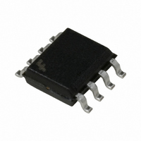
FDS3612 Fairchild Semiconductor, FDS3612 Datasheet - Page 2

FDS3612
Manufacturer Part Number
FDS3612
Description
MOSFET N-CH 100V 3.4A 8SOIC
Manufacturer
Fairchild Semiconductor
Series
PowerTrench®r
Datasheet
1.FDS3612.pdf
(5 pages)
Specifications of FDS3612
Fet Type
MOSFET N-Channel, Metal Oxide
Fet Feature
Logic Level Gate
Rds On (max) @ Id, Vgs
120 mOhm @ 3.4A, 10V
Drain To Source Voltage (vdss)
100V
Current - Continuous Drain (id) @ 25° C
3.4A
Vgs(th) (max) @ Id
4V @ 250µA
Gate Charge (qg) @ Vgs
20nC @ 10V
Input Capacitance (ciss) @ Vds
632pF @ 50V
Power - Max
1W
Mounting Type
Surface Mount
Package / Case
8-SOIC (3.9mm Width)
Lead Free Status / RoHS Status
Lead free / RoHS Compliant
Available stocks
Company
Part Number
Manufacturer
Quantity
Price
Part Number:
FDS3612
Manufacturer:
FAIRCHILD/ن»™ç«¥
Quantity:
20 000
Company:
Part Number:
FDS3612AZ_NL
Manufacturer:
FAIRCHILD
Quantity:
5 000
Company:
Part Number:
FDS3612_NL
Manufacturer:
FAIRCHILD
Quantity:
5 000
Notes:
1. R
Scale 1 : 1 on letter size paper
2. Pulse Test: Pulse Width < 300 s, Duty Cycle < 2.0%
Drain-Source Avalanche Ratings
W
I
Electrical Characteristics
Symbol
Off Characteristics
BV
I
I
I
On Characteristics
V
R
I
g
Dynamic Characteristics
C
C
C
Switching Characteristics
t
t
t
t
Q
Q
Q
Drain–Source Diode Characteristics and Maximum Ratings
I
V
the drain pins. R
AR
DSS
GSSF
GSSR
D(on)
d(on)
r
d(off)
f
S
BV
V
FS
GS(th)
SD
DS(on)
iss
oss
rss
g
gs
gd
DSS
JA
GS(th)
DSS
T
T
is the sum of the junction-to-case and case-to-ambient thermal resistance where the case thermal reference is defined as the solder mounting surface of
DSS
J
J
Drain-Source Avalanche Energy
Drain-Source Avalanche Current
Drain–Source Breakdown Voltage
Breakdown Voltage Temperature
Coefficient
Zero Gate Voltage Drain Current
Gate–Body Leakage, Forward
Gate–Body Leakage, Reverse
Gate Threshold Voltage
Gate Threshold Voltage
Temperature Coefficient
Static Drain–Source
On–Resistance
On–State Drain Current
Forward Transconductance
Input Capacitance
Output Capacitance
Reverse Transfer Capacitance
Turn–On Delay Time
Turn–On Rise Time
Turn–Off Delay Time
Turn–Off Fall Time
Total Gate Charge
Gate–Source Charge
Gate–Drain Charge
Maximum Continuous Drain–Source Diode Forward Current
Drain–Source Diode Forward
Voltage
JC
is guaranteed by design while R
a) 50°C/W (10 sec)
62.5°C/W steady state
when mounted on a
1in
copper
2
Parameter
pad of 2 oz
(Note 2)
(Note 2)
CA
is determined by the user's board design.
(Note 2)
Single Pulse, V
T
V
I
V
V
V
V
I
V
V
V
V
V
V
f = 1.0 MHz
V
V
V
V
V
A
D
D
= 25°C unless otherwise noted
GS
DS
GS
GS
DS
GS
GS
GS
GS
DS
DS
DD
GS
DS
GS
GS
= 250 A, Referenced to 25 C
= 250 A, Referenced to 25 C
b) 105°C/W when
= 10 V, I
= 80 V,
= V
= 10 V,
= 50 V,
= 50 V,
= 0 V,
= 20 V,
= –20 V,
= 10 V,
= 6 V,
= 10 V,
= 50 V,
= 10 V,
= 10 V
= 0 V,
mounted on a .04 in
pad of 2 oz copper
Test Conditions
GS
,
D
DD
= 3.4A, T
I
V
V
V
I
I
I
V
I
V
I
R
I
I
D
D
D
D
D
D
D
S
= 50 V, I
GS
DS
DS
DS
GEN
GS
= 250 A
= 250 A
= 3.4 A
= 3.2 A
= 3.4 A
= 1 A,
= 3.4 A,
= 2.1 A
= 0 V
= 0 V
= 10 V
= 0 V
= 0 V,
2
= 6
J
= 125 C
D
(Note 2)
= 3.4 A
Min
100
10
2
c) 125°C/W when mounted on a
Typ Max Units
0.75
106
170
632
minimum pad.
2.5
8.5
4.5
2.4
3.8
–6
88
94
11
40
20
23
14
2
–100
100
120
130
245
2.1
1.2
3.4
10
17
37
20
90
4
4
9
FDS3612 Rev B1(W)
mV/ C
mV/ C
m
nC
nC
nC
mJ
nA
nA
pF
pF
pF
ns
ns
ns
ns
V
V
A
S
A
V
A
A


