IRF5305S International Rectifier, IRF5305S Datasheet - Page 2
IRF5305S
Manufacturer Part Number
IRF5305S
Description
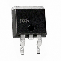
MOSFET P-CH 55V 31A D2PAK
Manufacturer
International Rectifier
Series
HEXFET®r
Datasheet
1.IRF5305S.pdf
(11 pages)
Specifications of IRF5305S
Fet Type
MOSFET P-Channel, Metal Oxide
Fet Feature
Standard
Rds On (max) @ Id, Vgs
60 mOhm @ 16A, 10V
Drain To Source Voltage (vdss)
55V
Current - Continuous Drain (id) @ 25° C
31A
Vgs(th) (max) @ Id
4V @ 250µA
Gate Charge (qg) @ Vgs
63nC @ 10V
Input Capacitance (ciss) @ Vds
1200pF @ 25V
Power - Max
3.8W
Mounting Type
Surface Mount
Package / Case
D²Pak, TO-263 (2 leads + tab)
Lead Free Status / RoHS Status
Contains lead / RoHS non-compliant
Other names
*IRF5305S
Available stocks
Company
Part Number
Manufacturer
Quantity
Price

Part Number:
IRF5305S
Manufacturer:
IR
Quantity:
20 000
Company:
Part Number:
IRF5305STRLPBF
Manufacturer:
IR
Quantity:
270 200
Company:
Part Number:
IRF5305STRLPBF
Manufacturer:
IR
Quantity:
20 000
Part Number:
IRF5305STRLPBF
Manufacturer:
IR
Quantity:
20 000
Company:
Part Number:
IRF5305STRPBF
Manufacturer:
IR
Quantity:
23 000
Company:
Part Number:
IRF5305STRRPBF
Manufacturer:
IR
Quantity:
23 000


IRF5305S/L
Electrical Characteristics @ T
Source-Drain Ratings and Characteristics
I
I
V
t
Q
t
I
I
L
S
V
R
V
g
Q
Q
Q
t
t
t
t
C
C
C
on
DSS
SM
rr
GSS
d(on)
d(off)
f
** When mounted on 1" square PCB (FR-4 or G-10 Material ).
r
S
SD
V
fs
Notes:
rr
(BR)DSS
DS(on)
GS(th)
g
gd
iss
oss
rss
gs
2
(BR)DSS
For recommended footprint and soldering techniques refer to application note #AN-994.
Repetitive rating; pulse width limited by
V
max. junction temperature. ( See fig. 11 )
R
T
I
SD
DD
J
G
= 25 , I
/ T
= -25V, Starting T
175°C
-16A, di/dt
J
Continuous Source Current
(Body Diode)
Pulsed Source Current
(Body Diode)
Diode Forward Voltage
Reverse Recovery Time
Reverse Recovery Charge
Forward Turn-On Time
Drain-to-Source Leakage Current
Internal Source Inductance
Drain-to-Source Breakdown Voltage
Breakdown Voltage Temp. Coefficient
Static Drain-to-Source On-Resistance
Gate Threshold Voltage
Forward Transconductance
Gate-to-Source Forward Leakage
Gate-to-Source Reverse Leakage
Total Gate Charge
Gate-to-Source Charge
Gate-to-Drain ("Miller") Charge
Turn-On Delay Time
Rise Time
Turn-Off Delay Time
Fall Time
Input Capacitance
Output Capacitance
Reverse Transfer Capacitance
AS
= -16A. (See Figure 12)
-280A/µs, V
J
Parameter
Parameter
= 25°C, L = 2.1mH
DD
V
(BR)DSS
J
= 25°C (unless otherwise specified)
,
Min. Typ. Max. Units
-2.0
Min. Typ. Max. Units
––– -0.034 –––
–––
–––
–––
–––
–––
–––
–––
–––
–––
–––
–––
–––
–––
–––
–––
–––
–––
–––
–––
–––
–––
-55
8.0
Uses IRF5305 data and test conditions
Pulse width
Intrinsic turn-on time is negligible (turn-on is dominated by L
1200 –––
–––
–––
–––
170
–––
––– 0.06
–––
–––
–––
––– -250
–––
––– -100
–––
–––
520
250
–––
71
14
39
63
7.5
66
-110
-1.3
110
250
-4.0
100
–––
–––
–––
–––
–––
–––
–––
–––
–––
-31
-25
63
13
29
300µs; duty cycle
V/°C
nC
ns
µA
nA
ns
nH
nC
V
pF
A
V
V
S
MOSFET symbol
showing the
p-n junction diode.
T
T
di/dt = -100A/µs
integral reverse
V
Reference to 25°C, I
V
V
V
V
V
V
V
I
V
V
R
R
Between lead,
and center of die contact
V
ƒ = 1.0MHz, See Fig. 5
V
I
V
D
D
J
J
GS
GS
DS
DS
DS
DS
GS
GS
DS
GS
DD
GS
DS
G
D
= 25°C, I
= 25°C, I
= -16A
= -16A
= 6.8
= 1.6
= V
= -44V, V
= 0V, I
= -10V, I
= -25V, I
= -55V, V
= 20V
= -20V
= -44V
= -10V, See Fig. 6 and 13
= 0V
= -25V
= -28V
GS
2%.
, I
F
See Fig. 10
S
D
D
= -16A
Conditions
= -16A, V
= -250µA
D
D
GS
Conditions
GS
= -250µA
= -16A
= -16A
= 0V, T
= 0V
D
www.irf.com
= -1mA
GS
G
J
= 0V
= 150°C
S
+L
D
S
D
)
Related parts for IRF5305S
Image
Part Number
Description
Manufacturer
Datasheet
Request
R

Part Number:
Description:
SCHOTTKY RECTIFIER
Manufacturer:
International Rectifier Corp.
Datasheet:
Part Number:
Description:
SCHOTTKY RECTIFIER
Manufacturer:
International Rectifier Corp.
Datasheet:
Part Number:
Description:
SCHOTTKY RECTIFIER
Manufacturer:
International Rectifier Corp.
Datasheet:
Part Number:
Description:
SCHOTTKY RECTIFIER
Manufacturer:
International Rectifier Corp.
Datasheet:
Part Number:
Description:
SCHOTTKY RECTIFIER
Manufacturer:
International Rectifier Corp.
Datasheet:
Part Number:
Description:
SCHOTTKY RECTIFIER
Manufacturer:
International Rectifier Corp.
Datasheet:
Part Number:
Description:
SCHOTTKY RECTIFIER
Manufacturer:
International Rectifier Corp.
Datasheet:
Part Number:
Description:
SCHOTTKY RECTIFIER
Manufacturer:
International Rectifier Corp.
Datasheet:
Part Number:
Description:
SCHOTTKY RECTIFIER
Manufacturer:
International Rectifier Corp.
Datasheet:
Part Number:
Description:
SCHOTTKY RECTIFIER
Manufacturer:
International Rectifier Corp.
Datasheet:
Part Number:
Description:
SCHOTTKY RECTIFIER
Manufacturer:
International Rectifier Corp.
Datasheet:
Part Number:
Description:
SCHOTTKY RECTIFIER
Manufacturer:
International Rectifier Corp.
Datasheet:
Part Number:
Description:
SCHOTTKY RECTIFIER
Manufacturer:
International Rectifier Corp.
Datasheet:
Part Number:
Description:
SCHOTTKY RECTIFIER
Manufacturer:
International Rectifier Corp.
Datasheet:
Part Number:
Description:
SCHOTTKY RECTIFIER
Manufacturer:
International Rectifier Corp.
Datasheet: