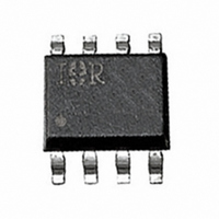
IRF7433 International Rectifier, IRF7433 Datasheet

IRF7433
Specifications of IRF7433
Available stocks
Related parts for IRF7433
IRF7433 Summary of contents
Page 1
... Linear Derating Factor V Gate-to-Source Voltage Junction and Storage Temperature Range J STG Thermal Resistance Parameter R Maximum Junction-to-Ambient JA www.irf.com HEXFET V DSS -12V -4. -4.5V GS ƒ ƒ ƒ PD -94056 IRF7433 ® Power MOSFET R max I DS(on) D 24m @V = -4.5V 8. 30m @V = -2.5V 7. 46m @V = -1.8V 6. SO-8 Max. Units - ...
Page 2
... IRF7433 Electrical Characteristics @ T Parameter V Drain-to-Source Breakdown Voltage (BR)DSS Breakdown Voltage Temp. Coefficient (BR)DSS J R Static Drain-to-Source On-Resistance DS(on) V Gate Threshold Voltage GS(th) g Forward Transconductance fs I Drain-to-Source Leakage Current DSS Gate-to-Source Forward Leakage I GSS Gate-to-Source Reverse Leakage Q Total Gate Charge g Q Gate-to-Source Charge ...
Page 3
... BOTTOM -1.2V 1 0.1 10 100 0.1 Fig 2. Typical Output Characteristics 2 1.5 1.0 0.5 = -10V DS 0.0 2.0 2.5 -60 -40 -20 Fig 4. Normalized On-Resistance IRF7433 VGS TOP -10.0V -7.0V -4.5V -3.0V -2.5V -1.8V -1.5V BOTTOM -1.2V -1.2V 20µs PULSE WIDTH Tj = 150° Drain-to-Source Voltage (V) -8. ...
Page 4
... IRF7433 3200 0V MHZ C iss = SHORTED 2800 C rss = C gd 2400 C oss = Ciss 2000 1600 1200 Coss 800 Crss 400 Drain-to-Source Voltage (V) Fig 5. Typical Capacitance Vs. Drain-to-Source Voltage 100 150 C ° 0.1 0.2 0.4 0.6 0.8 -V ,Source-to-Drain Voltage (V) SD Fig 7. Typical Source-Drain Diode Forward Voltage ...
Page 5
... Fig 11. Maximum Effective Transient Thermal Impedance, Junction-to-Ambient www.irf.com Pulse Width Duty Factor Fig 10a. Switching Time Test Circuit t d(on 10% 125 150 ° 90 Fig 10b. Switching Time Waveforms Notes: 1. Duty factor Peak 0.01 0 Rectangular Pulse Duration (sec) 1 IRF7433 D.U. µ d(off thJA ...
Page 6
... IRF7433 0.050 0.040 0.030 -8.7A 0.020 0.010 0.0 2.0 4.0 -V GS, Gate -to -Source Voltage (V) Fig 12. Typical On-Resistance Vs. Gate Voltage Charge Fig 14a. Basic Gate Charge Waveform 6 0.15 0.12 0.09 0.06 0.03 0 6.0 8.0 10.0 0.0 5.0 10.0 15.0 20.0 25.0 30.0 35.0 40.0 Fig 13 ...
Page 7
... Temperature ( °C ) Fig 15. Typical Vgs(th) Vs. Junction Temperature www.irf.com 300 200 -250µA 100 0 75 100 125 150 0.0001 0.0010 0.0100 0.1000 1.0000 10.0000 100.0000 Fig 16. Typical Power Vs. Time IRF7433 Time (sec) 7 ...
Page 8
... IRF7433 SO-8 Package Details 0.25 [.010 NOT DIMENSIONING & T OLERANCING PER AS ME Y14.5M-1994. 2. CONT ROLLING DIMENS ION: MILLIMET ER 3. DIMENSIONS ARE SHOWN IN MILLIMETERS [INCHES ]. 4. OUTLINE CONFORMS T O JEDEC OUTLINE MS-012AA. 5 DIMENSION DOES NOT INCLUDE MOLD PROT RUSIONS. MOLD PROTRUS IONS NOT TO EXCEED 0.15 [.006]. ...
Page 9
... This product has been designed and qualified for the commercial market. IR WORLD HEADQUARTERS: 233 Kansas St., El Segundo, California 90245, USA Tel: (310) 252-7105 www.irf.com 0 Data and specifications subject to change without notice. Qualification Standards can be found on IR’s Web site. Visit us at www.irf.com for sales contact information.12/00 IRF7433 . . TAC Fax: (310) 252-7903 9 ...


