IRF1010EZ International Rectifier, IRF1010EZ Datasheet - Page 2
IRF1010EZ
Manufacturer Part Number
IRF1010EZ
Description
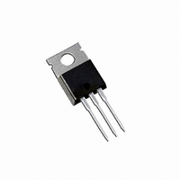
MOSFET N-CH 60V 75A TO-220AB
Manufacturer
International Rectifier
Series
HEXFET®r
Datasheet
1.IRF1010EZL.pdf
(12 pages)
Specifications of IRF1010EZ
Fet Type
MOSFET N-Channel, Metal Oxide
Fet Feature
Standard
Rds On (max) @ Id, Vgs
8.5 mOhm @ 51A, 10V
Drain To Source Voltage (vdss)
60V
Current - Continuous Drain (id) @ 25° C
75A
Vgs(th) (max) @ Id
4V @ 100µA
Gate Charge (qg) @ Vgs
86nC @ 10V
Input Capacitance (ciss) @ Vds
2810pF @ 25V
Power - Max
140W
Mounting Type
Through Hole
Package / Case
TO-220-3 (Straight Leads)
Lead Free Status / RoHS Status
Contains lead / RoHS non-compliant
Other names
*IRF1010EZ
Available stocks
Company
Part Number
Manufacturer
Quantity
Price
Company:

Part Number:
IRF1010EZ
Manufacturer:
IR
Quantity:
12 500
Part Number:
IRF1010EZ
Manufacturer:
IR
Quantity:
20 000
Company:
Part Number:
IRF1010EZL
Manufacturer:
IR
Quantity:
12 500
Part Number:
IRF1010EZLPBF
Manufacturer:
IR
Quantity:
20 000
Part Number:
IRF1010EZPBF
Manufacturer:
VISHAY/威世
Quantity:
20 000
Company:
Part Number:
IRF1010EZS
Manufacturer:
IR
Quantity:
12 500
Part Number:
IRF1010EZS
Manufacturer:
IR
Quantity:
20 000


‚
ƒ
„
V
R
V
gfs
I
I
Q
Q
Q
t
t
t
t
L
L
C
C
C
C
C
C
I
I
V
t
Q
t
Static @ T
Diode Characteristics
DSS
GSS
d(on)
r
d(off)
f
S
SM
rr
on
D
S
(BR)DSS
GS(th)
SD
2
DS(on)
g
gs
gd
iss
oss
rss
oss
oss
oss
rr
Repetitive rating; pulse width limited by
I
Pulse width
V
max. junction temperature. (See fig. 11).
R
recommended for use above this value.
T
Limited by T
SD
J
DSS
G
eff.
= 25 , I
/ T
175°C.
51A, di/dt
J
AS
J
Jmax
Drain-to-Source Breakdown Voltage
Breakdown Voltage Temp. Coefficient –––
Static Drain-to-Source On-Resistance –––
Gate Threshold Voltage
Forward Transconductance
Drain-to-Source Leakage Current
Gate-to-Source Forward Leakage
Gate-to-Source Reverse Leakage
Total Gate Charge
Gate-to-Source Charge
Gate-to-Drain ("Miller") Charge
Turn-On Delay Time
Rise Time
Turn-Off Delay Time
Fall Time
Internal Drain Inductance
Internal Source Inductance
Input Capacitance
Output Capacitance
Reverse Transfer Capacitance
Output Capacitance
Output Capacitance
Effective Output Capacitance
Continuous Source Current
(Body Diode)
Pulsed Source Current
(Body Diode)
Diode Forward Voltage
Reverse Recovery Time
Reverse Recovery Charge
Forward Turn-On Time
1.0ms; duty cycle
= 51A, V
= 25°C (unless otherwise specified)
, starting T
260A/µs, V
Parameter
GS
Parameter
=10V. Part not
J
™
DD
= 25°C, L = 0.077mH,
V
2%.
(BR)DSS
,
Intrinsic turn-on time is negligible (turn-on is dominated by LS+LD)
Min. Typ. Max. Units
Min. Typ. Max. Units
…
†
‡
ˆ
200
–––
–––
–––
–––
–––
–––
–––
–––
–––
–––
–––
–––
–––
–––
–––
–––
–––
–––
–––
–––
–––
–––
–––
–––
2.0
60
C
as C
Limited by T
avalanche performance.
This value determined from sample failure population. 100%
tested to this value in production.
This is applied to D
( FR-4 or G-10 Material ). For recommended footprint and
soldering techniques refer to application note #AN-994.
oss
0.058
2810
1440
oss
–––
–––
–––
–––
–––
–––
–––
420
200
320
510
–––
–––
–––
eff. is a fixed capacitance that gives the same charging time
6.8
4.5
7.5
58
19
21
19
90
38
54
41
54
while V
-200
–––
–––
–––
250
200
–––
–––
–––
–––
–––
–––
–––
–––
–––
–––
–––
–––
340
Jmax
8.5
4.0
1.3
20
86
28
32
84
62
81
DS
, see Fig.12a, 12b, 15, 16 for typical repetitive
is rising from 0 to 80% V
2
V/°C
m
Pak, when mounted on 1" square PCB
µA
nA
nC
nH
nC
pF
ns
ns
V
V
S
A
V
V
Reference to 25°C, I
V
V
V
V
V
V
V
I
V
V
V
I
R
V
Between lead,
6mm (0.25in.)
from package
and center of die contact
V
V
ƒ = 1.0MHz, See Fig. 5
V
V
V
MOSFET symbol
showing the
integral reverse
p-n junction diode.
T
T
di/dt = 100A/µs
D
D
J
J
GS
GS
DS
DS
DS
DS
GS
GS
DS
GS
DD
GS
GS
DS
GS
GS
GS
G
= 51A
= 51A
= 25°C, I
= 25°C, I
= 7.95
= 0V, I
= 10V, I
= V
= 25V, I
= 60V, V
= 60V, V
= 20V
= -20V
= 48V
= 10V
= 30V
= 10V
= 0V
= 25V
= 0V, V
= 0V, V
= 0V, V
GS
, I
D
f
f
Conditions
Conditions
D
DS
S
F
D
D
DS
DS
= 250µA
GS
GS
= 100µA
= 51A, V
= 51A, V
= 51A
= 51A
= 0V to 48V
= 1.0V, ƒ = 1.0MHz
= 48V, ƒ = 1.0MHz
= 0V
= 0V, T
f
DSS
www.irf.com
.
f
D
= 1mA
DD
GS
J
G
= 125°C
= 30V
= 0V
G
f
S
D
D
S
Related parts for IRF1010EZ
Image
Part Number
Description
Manufacturer
Datasheet
Request
R

Part Number:
Description:
SCHOTTKY RECTIFIER
Manufacturer:
International Rectifier Corp.
Datasheet:
Part Number:
Description:
SCHOTTKY RECTIFIER
Manufacturer:
International Rectifier Corp.
Datasheet:
Part Number:
Description:
SCHOTTKY RECTIFIER
Manufacturer:
International Rectifier Corp.
Datasheet:
Part Number:
Description:
SCHOTTKY RECTIFIER
Manufacturer:
International Rectifier Corp.
Datasheet:
Part Number:
Description:
SCHOTTKY RECTIFIER
Manufacturer:
International Rectifier Corp.
Datasheet:
Part Number:
Description:
SCHOTTKY RECTIFIER
Manufacturer:
International Rectifier Corp.
Datasheet:
Part Number:
Description:
SCHOTTKY RECTIFIER
Manufacturer:
International Rectifier Corp.
Datasheet:
Part Number:
Description:
SCHOTTKY RECTIFIER
Manufacturer:
International Rectifier Corp.
Datasheet:
Part Number:
Description:
SCHOTTKY RECTIFIER
Manufacturer:
International Rectifier Corp.
Datasheet:
Part Number:
Description:
SCHOTTKY RECTIFIER
Manufacturer:
International Rectifier Corp.
Datasheet:
Part Number:
Description:
SCHOTTKY RECTIFIER
Manufacturer:
International Rectifier Corp.
Datasheet:
Part Number:
Description:
SCHOTTKY RECTIFIER
Manufacturer:
International Rectifier Corp.
Datasheet:
Part Number:
Description:
SCHOTTKY RECTIFIER
Manufacturer:
International Rectifier Corp.
Datasheet:
Part Number:
Description:
SCHOTTKY RECTIFIER
Manufacturer:
International Rectifier Corp.
Datasheet:
Part Number:
Description:
SCHOTTKY RECTIFIER
Manufacturer:
International Rectifier Corp.
Datasheet: