SPD07N60S5 Infineon Technologies, SPD07N60S5 Datasheet - Page 2
SPD07N60S5
Manufacturer Part Number
SPD07N60S5
Description
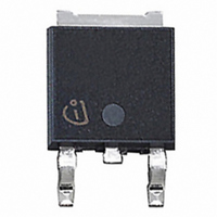
MOSFET N-CH 600V 7.3A DPAK
Manufacturer
Infineon Technologies
Series
CoolMOS™r
Datasheet
1.SPD07N60S5.pdf
(12 pages)
Specifications of SPD07N60S5
Package / Case
DPak, TO-252 (2 leads+tab), SC-63
Fet Type
MOSFET N-Channel, Metal Oxide
Fet Feature
Standard
Rds On (max) @ Id, Vgs
600 mOhm @ 4.6A, 10V
Drain To Source Voltage (vdss)
600V
Current - Continuous Drain (id) @ 25° C
7.3A
Vgs(th) (max) @ Id
5.5V @ 350µA
Gate Charge (qg) @ Vgs
35nC @ 10V
Input Capacitance (ciss) @ Vds
970pF @ 25V
Power - Max
83W
Mounting Type
Surface Mount
Minimum Operating Temperature
- 55 C
Configuration
Single
Transistor Polarity
N-Channel
Resistance Drain-source Rds (on)
0.6 Ohm @ 10 V
Drain-source Breakdown Voltage
600 V
Gate-source Breakdown Voltage
+/- 20 V
Continuous Drain Current
7.3 A
Power Dissipation
83000 mW
Maximum Operating Temperature
+ 150 C
Mounting Style
SMD/SMT
Lead Free Status / RoHS Status
Contains lead / RoHS non-compliant
Lead Free Status / RoHS Status
Lead free / RoHS Compliant, Contains lead / RoHS non-compliant
Other names
SP000313948
SPD07N60S5INTR
SPD07N60S5INTR
Available stocks
Company
Part Number
Manufacturer
Quantity
Price
Company:

Part Number:
SPD07N60S5
Manufacturer:
infineon
Quantity:
410
Company:
Part Number:
SPD07N60S5
Manufacturer:
INFINEON
Quantity:
30 000
Company:
Part Number:
SPD07N60S5
Manufacturer:
INFINEON
Quantity:
731


*) TO252: reflow soldering, MSL3; TO251: wavesoldering
Maximum Ratings
Parameter
Drain Source voltage slope
V
Thermal Characteristics
Parameter
Thermal resistance, junction - case
Thermal resistance, junction - ambient, leaded
SMD version, device on PCB:
@ min. footprint
@ 6 cm
Soldering temperature, *)
1.6 mm (0.063 in.) from case for 10s
Electrical Characteristics, at T j=25°C unless otherwise specified
Parameter
Drain-source breakdown voltage V
Drain-Source avalanche
breakdown voltage
Gate threshold voltage
Zero gate voltage drain current
Gate-source leakage current
Drain-source on-state resistance R
Gate input resistance
Rev. 2.5
DS
= 480 V, I
2
cooling area
D
= 7.3 A, T
j
2)
= 125 °C
V
V
I
I
R
Symbol
DSS
GSS
(BR)DSS V
(BR)DS
GS(th)
DS(on)
G
Page 2
V
I
V
T
T
V
V
T
T
f =1MHz, open Drain
D
j
j
j
j
GS
GS
DS
GS
GS
=25°C,
=150°C
=25°C
=150°C
=350 µΑ , V
Conditions
=600V, V
=0V, I
=0V, I
=20V, V
=10V, I
Symbol
d v /d t
Symbol
R
R
R
T
D
D
=0.25mA
=7.3A
sold
thJC
thJA
thJA
D
DS
GS
GS
=4.6A,
=0V
=V
=0V,
DS
min.
min.
600
3.5
-
-
-
-
-
-
-
-
-
-
-
-
Values
Values
Value
0.54
1.46
typ.
typ.
700
4.5
0.5
20
19
-
-
-
-
-
-
-
-
SPU07N60S5
SPD07N60S5
2008-04-10
max.
max.
260
100
100
1.5
5.5
0.6
75
75
50
1
-
-
-
-
Unit
V/ns
Unit
K/W
°C
Unit
V
µA
nA
Ω
Related parts for SPD07N60S5
Image
Part Number
Description
Manufacturer
Datasheet
Request
R

Part Number:
Description:
Manufacturer:
Infineon Technologies AG
Datasheet:
Part Number:
Description:
Manufacturer:
Infineon Technologies AG
Datasheet:
Part Number:
Description:
Manufacturer:
Infineon Technologies AG
Datasheet:
Part Number:
Description:
Manufacturer:
Infineon Technologies AG
Datasheet:
Part Number:
Description:
Manufacturer:
Infineon Technologies AG
Datasheet:
Part Number:
Description:
Manufacturer:
Infineon Technologies AG
Datasheet:
Part Number:
Description:
Manufacturer:
Infineon Technologies AG
Datasheet:
Part Number:
Description:
16-bit microcontroller with 2x2 KByte RAM
Manufacturer:
Infineon Technologies AG
Datasheet:
Part Number:
Description:
NPN silicon RF transistor
Manufacturer:
Infineon Technologies AG
Datasheet:
Part Number:
Description:
NPN silicon RF transistor
Manufacturer:
Infineon Technologies AG
Datasheet:
Part Number:
Description:
NPN silicon RF transistor
Manufacturer:
Infineon Technologies AG
Datasheet:
Part Number:
Description:
NPN silicon RF transistor
Manufacturer:
Infineon Technologies AG
Datasheet:
Part Number:
Description:
Si-MMIC-amplifier in SIEGET 25-technologie
Manufacturer:
Infineon Technologies AG
Datasheet:
Part Number:
Description:
IGBT Power Module
Manufacturer:
Infineon Technologies AG
Datasheet:
Part Number:
Description:
IC for switching-mode power supplies
Manufacturer:
Infineon Technologies AG
Datasheet: