MTD6N15T4 ON Semiconductor, MTD6N15T4 Datasheet - Page 4
MTD6N15T4
Manufacturer Part Number
MTD6N15T4
Description
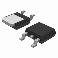
MOSFET N-CH 150V 6A DPAK
Manufacturer
ON Semiconductor
Datasheet
1.MTD6N15T4G.pdf
(6 pages)
Specifications of MTD6N15T4
Fet Type
MOSFET N-Channel, Metal Oxide
Fet Feature
Standard
Rds On (max) @ Id, Vgs
300 mOhm @ 3A, 10V
Drain To Source Voltage (vdss)
150V
Current - Continuous Drain (id) @ 25° C
6A
Vgs(th) (max) @ Id
4.5V @ 1mA
Gate Charge (qg) @ Vgs
30nC @ 10V
Input Capacitance (ciss) @ Vds
1200pF @ 25V
Power - Max
1.25W
Mounting Type
Surface Mount
Package / Case
DPak, TO-252 (2 leads+tab), SC-63
Lead Free Status / RoHS Status
Contains lead / RoHS non-compliant
Other names
MTD6N15T4OSCT
Available stocks
Company
Part Number
Manufacturer
Quantity
Price
Company:

Part Number:
MTD6N15T4
Manufacturer:
MOT/ON
Quantity:
12 500
Part Number:
MTD6N15T4
Manufacturer:
ON/安森美
Quantity:
20 000
Company:
Part Number:
MTD6N15T4G
Manufacturer:
ON
Quantity:
12 500
Part Number:
MTD6N15T4G
Manufacturer:
ON/安森美
Quantity:
20 000


FORWARD BIASED SAFE OPERATING AREA
voltage and drain current that a device can safely handle
when it is forward biased, or when it is on, or being turned
on. Because these curves include the limitations of
simultaneous high voltage and high current, up to the rating
of the device, they are especially useful to designers of linear
systems. The curves are based on a case temperature of 25°C
and a maximum junction temperature of 150°C. Limitations
for repetitive pulses at various case temperatures can be
determined by using the thermal response curves. Motorola
Application
Resistance−General Data and Its Use” provides detailed
instructions.
0.05
0.03
The FBSOA curves define the maximum drain−to−source
0.5
0.2
0.1
20
10
5
2
1
0.07
0.05
0.03
0.02
0.01
0.3 0.5 0.7
0.7
0.5
0.3
0.2
0.1
0.01
Figure 8. Maximum Rated Forward Biased
0.05
0.02
D = 0.5
0.2
0.1
0.01
0.02 0.03
T
V
V
C
DS
GS
Note,
1
= 25°C
, DRAIN−TO−SOURCE VOLTAGE (VOLTS)
= 20 V SINGLE PULSE
SINGLE PULSE
2
Safe Operating Area
3
0.05
10 ms
AN569,
R
THERMAL LIMIT
PACKAGE LIMIT
DS(on)
5
7
0.1
LIMIT
10
1 ms
20
“Transient
100 ms
0.2 0.3
30
50
dc
10 ms
70
Figure 10. Thermal Response
0.5
SAFE OPERATING AREA
100
Thermal
t, TIME OR PULSE WIDTH (ms)
http://onsemi.com
200
1
MTD6N15
300
2
4
3
SWITCHING SAFE OPERATING AREA
boundary that the load line may traverse without incurring
damage to the MOSFET. The fundamental limits are the
peak current, I
The switching SOA shown in Figure 8 is applicable for both
turn−on and turn−off of the devices for switching times less
than one microsecond.
must be less than:
20
15
10
The switching safe operating area (SOA) of Figure 9 is the
The power averaged over a complete switching cycle
5
0
P
0
(pk)
5
DUTY CYCLE, D = t
t
1
20
10
Figure 9. Maximum Rated Switching
t
V
2
T
DS
J
DM
, DRAIN−TO−SOURCE VOLTAGE (VOLTS)
≤ 150°C
40
20
and the breakdown voltage, V
Safe Operating Area
1
/t
T
2
60
J(max)
50
R
R
R
D CURVES APPLY FOR POWER
PULSE TRAIN SHOWN
READ TIME AT t
T
qJC
J(pk)
qJC
qJC
80
− T
(t) = r(t) R
(t) = 6.25°C/W MAX
− T
100
C
C
100
= P
qJC
(pk)
200
1
R
120
qJC
(t)
500
140
(BR)DSS
1000
160
.
Related parts for MTD6N15T4
Image
Part Number
Description
Manufacturer
Datasheet
Request
R

Part Number:
Description:
ON Semiconductor [VOLTAGE REGULATOR]
Manufacturer:
ON Semiconductor
Datasheet:
Part Number:
Description:
357-036-542-201 CARDEDGE 36POS DL .156 BLK LOPRO
Manufacturer:
ON Semiconductor
Datasheet:
Part Number:
Description:
357-036-542-201 CARDEDGE 36POS DL .156 BLK LOPRO
Manufacturer:
ON Semiconductor
Datasheet:
Part Number:
Description:
357-036-542-201 CARDEDGE 36POS DL .156 BLK LOPRO
Manufacturer:
ON Semiconductor
Datasheet:
Part Number:
Description:
357-036-542-201 CARDEDGE 36POS DL .156 BLK LOPRO
Manufacturer:
ON Semiconductor
Datasheet:
Part Number:
Description:
357-036-542-201 CARDEDGE 36POS DL .156 BLK LOPRO
Manufacturer:
ON Semiconductor
Datasheet:
Part Number:
Description:
357-036-542-201 CARDEDGE 36POS DL .156 BLK LOPRO
Manufacturer:
ON Semiconductor
Datasheet:
Part Number:
Description:
357-036-542-201 CARDEDGE 36POS DL .156 BLK LOPRO
Manufacturer:
ON Semiconductor
Datasheet:
Part Number:
Description:
357-036-542-201 CARDEDGE 36POS DL .156 BLK LOPRO
Manufacturer:
ON Semiconductor
Datasheet:
Part Number:
Description:
357-036-542-201 CARDEDGE 36POS DL .156 BLK LOPRO
Manufacturer:
ON Semiconductor
Datasheet:
Part Number:
Description:
357-036-542-201 CARDEDGE 36POS DL .156 BLK LOPRO
Manufacturer:
ON Semiconductor
Datasheet:
Part Number:
Description:
Manufacturer:
ON Semiconductor
Datasheet:
Part Number:
Description:
Manufacturer:
ON Semiconductor
Datasheet:
Part Number:
Description:
Manufacturer:
ON Semiconductor
Datasheet: