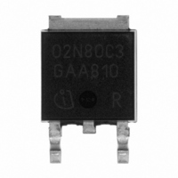
SPD02N80C3 Infineon Technologies, SPD02N80C3 Datasheet

SPD02N80C3
Manufacturer Part Number
SPD02N80C3
Description
MOSFET N-CH 800V 2A TO-252
Manufacturer
Infineon Technologies
Series
CoolMOS™r
Specifications of SPD02N80C3
Package / Case
DPak, TO-252 (2 leads+tab), SC-63
Fet Type
MOSFET N-Channel, Metal Oxide
Fet Feature
Standard
Rds On (max) @ Id, Vgs
2.7 Ohm @ 1.2A, 10V
Drain To Source Voltage (vdss)
800V
Current - Continuous Drain (id) @ 25° C
2A
Vgs(th) (max) @ Id
3.9V @ 120µA
Gate Charge (qg) @ Vgs
16nC @ 10V
Input Capacitance (ciss) @ Vds
290pF @ 100V
Power - Max
42W
Mounting Type
Surface Mount
Minimum Operating Temperature
- 55 C
Configuration
Single
Transistor Polarity
N-Channel
Resistance Drain-source Rds (on)
2.7 Ohm @ 10 V
Drain-source Breakdown Voltage
800 V
Gate-source Breakdown Voltage
+/- 20 V
Continuous Drain Current
2 A
Power Dissipation
42000 mW
Maximum Operating Temperature
+ 150 C
Mounting Style
SMD/SMT
Continuous Drain Current Id
2A
Drain Source Voltage Vds
800V
On Resistance Rds(on)
2.7ohm
Rds(on) Test Voltage Vgs
10V
Threshold Voltage Vgs Typ
3V
Rohs Compliant
Yes
Lead Free Status / RoHS Status
Lead free / RoHS Compliant
Lead Free Status / RoHS Status
Lead free / RoHS Compliant, Lead free / RoHS Compliant
Other names
SP000014822
SP000315409
SPD02N80C3
SPD02N80C3INTR
SPD02N80C3XT
SP000315409
SPD02N80C3
SPD02N80C3INTR
SPD02N80C3XT
Available stocks
Company
Part Number
Manufacturer
Quantity
Price
Company:
Part Number:
SPD02N80C3
Manufacturer:
Infineon Technologies
Quantity:
34 817
Part Number:
SPD02N80C3
Manufacturer:
INFINEON/英飞凌
Quantity:
20 000
T
T
Gate source voltage
Rev. 2.5
C
C
V
V
DD
DD
G
t
p
T
jmax
Page
T
T
jmax
jmax
E
V
V
P
AR
GS
GS
tot
V
DS
G
2008-04-11
Related parts for SPD02N80C3
SPD02N80C3 Summary of contents
Page 1
Gate source voltage Rev. 2.5 T jmax jmax T jmax tot Page 2008-04-11 ...
Page 2
reflow soldering, MSL3 Rev. 2.5 R thJC V (BR)DSS ...
Page 3
Transconductance Input capacitance Output capacitance Reverse transfer capacitance Turn-on delay time Rise time Turn-off delay time Fall time Gate to source charge Gate to drain charge Rev. 2 iss GS DS ...
Page 4
Inverse diode direct current, pulsed Reverse recovery time Reverse recovery charge Peak reverse recovery current Rev rrm 2008-04-11 ...
Page 5
Rev. 2 2008-04-11 ...
Page 6
Rev. 2 2008-04-11 ...
Page 7
max V DS max Rev. 2 2008-04-11 ...
Page 8
(BR)DSS j Rev. 2 2008-04-11 ...
Page 9
iss C oss C rss Rev. 2.5 C oss 2008-04-11 ...
Page 10
PG-TO252-3-11, PG-TO252-3-21 G Rev. 2.5 2008-04-11 ...
Page 11
Rev. 2.5 2008-04-11 ...


