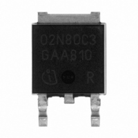
SPD02N80C3 Infineon Technologies, SPD02N80C3 Datasheet

MOSFET N-CH 800V 2A TO-252

SPD02N80C3

Manufacturer Part Number
SPD02N80C3
Description
MOSFET N-CH 800V 2A TO-252
Manufacturer
Infineon Technologies
Series
CoolMOS™r
Datasheets

Specifications of SPD02N80C3

Package / Case
DPak, TO-252 (2 leads+tab), SC-63
Fet Type
MOSFET N-Channel, Metal Oxide
Fet Feature
Standard
Rds On (max) @ Id, Vgs
2.7 Ohm @ 1.2A, 10V
Drain To Source Voltage (vdss)
800V
Current - Continuous Drain (id) @ 25° C
2A
Vgs(th) (max) @ Id
3.9V @ 120µA
Gate Charge (qg) @ Vgs
16nC @ 10V
Input Capacitance (ciss) @ Vds
290pF @ 100V
Power - Max
42W
Mounting Type
Surface Mount
Minimum Operating Temperature
- 55 C
Configuration
Single
Transistor Polarity
N-Channel
Resistance Drain-source Rds (on)
2.7 Ohm @ 10 V
Drain-source Breakdown Voltage
800 V
Gate-source Breakdown Voltage
+/- 20 V
Continuous Drain Current
2 A
Power Dissipation
42000 mW
Maximum Operating Temperature
+ 150 C
Mounting Style
SMD/SMT
Continuous Drain Current Id
2A
Drain Source Voltage Vds
800V
On Resistance Rds(on)
2.7ohm
Rds(on) Test Voltage Vgs
10V
Threshold Voltage Vgs Typ
3V
Rohs Compliant
Yes
Lead Free Status / RoHS Status
Lead free / RoHS Compliant
Lead Free Status / RoHS Status
Lead free / RoHS Compliant, Lead free / RoHS Compliant
Other names
SP000014822
SP000315409
SPD02N80C3
SPD02N80C3INTR
SPD02N80C3XT

Available stocks

Company
Part Number
Manufacturer
Quantity
Price
Part Number:
SPD02N80C3
Manufacturer:
Infineon Technologies
Quantity:
34 817
Part Number:
SPD02N80C3
Manufacturer:
INFINEON/英飞凌
Quantity:
20 000
Part Number:
SPD02N80C3
0
Company:
Part Number:
SPD02N80C3
Quantity:
2 500
Rev. 2.9
Features
• New revolutionary high voltage technology
• Extreme dv/dt rated
• High peak current capability
• Qualified according to JEDEC
• Pb-free lead plating; RoHS compliant
• Ultra low gate charge
• Ultra low effective capacitances
CoolMOS
• Industrial application with high DC bulk voltage
• Switching Application ( i.e. active clamp forward )
Maximum ratings, at T
Parameter
Continuous drain current
Pulsed drain current
Avalanche energy, single pulse
Avalanche energy, repetitive t
Avalanche current, repetitive t
MOSFET dv /dt ruggedness
Gate source voltage
Power dissipation
Operating and storage temperature
CoolMOS
Type
SPD02N80C3
TM
TM
800V designed for:
Power Transistor
2)
Package
PG-TO252-3
j
=25 °C, unless otherwise specified
AR
AR
1)
2),3)
2),3)
for target applications
Symbol Conditions
I
I
E
E
I
dv /dt
V
P
T
D
D,pulse
AR
Marking
02N80C3
j
AS
AR
GS
tot
, T
stg
T
T
T
I
I
V
static
AC (f >1 Hz)
T
D
D
page 1
C
C
C
C
DS
=1 A, V
=2 A, V
=25 °C
=100 °C
=25 °C
=25 °C
=0…640 V
DD
DD
=50 V
=50 V
Product Summary
V
R
Q
DS
DS(on)max
g,typ
@ T
j
= 25°C
-55 ... 150
Value
PG-TO252-3
0.05
±20
±30
1.2
90
50
42
2
6
2
SPD02N80C3
800
2.7
12
Unit
A
mJ
A
V/ns
V
W
°C
Ω
V
nC
2008-10-15

Related parts for SPD02N80C3

SPD02N80C3 Summary of contents

Page 1

... DS R DS(on)max Q g,typ 1) for target applications Marking 02N80C3 Symbol Conditions =25 ° =100 ° =25 ° D,pulse = 2), = 2), =0…640 static >1 Hz) =25 ° tot stg page 1 SPD02N80C3 800 25°C 2.7 Ω PG-TO252-3 Value Unit V/ns ±20 V ± -55 ... 150 °C 2008-10-15 ...

Page 2

... I =0. GS(th =800 DSS =25 ° =800 =150 ° = GSS DS(on) =25 ° = =1 =150 ° MHz, open drain R G page 2 SPD02N80C3 Value Unit V/ns Values Unit min. typ. max K 260 °C 800 - - V - 870 - 2 µ 100 nA Ω - 2.4 2.7 - 6.5 - Ω ...

Page 3

... T =25 °C R d(off =640 plateau = =25 ° =400 /dt =100 A/µ rrm < <T , identical low side and high side switch peak (BR)DSS j jmax while V oss DS while V oss DS page 3 SPD02N80C3 Values Unit min. typ. max. - 290 - 520 - µ * rising from 0 to 80% V DSS ...

Page 4

... Rev. 2.9 2 Safe operating area =f parameter 100 125 150 [° Typ. output characteristics =f parameter [s] p page 4 SPD02N80C3 ); T =25 ° limited by on-state resistance 10 µs 100 µ 100 V [ =25 °C; t =10 µ µs 1000 25 2008-10-15 ...

Page 5

... T Rev. 2.9 6 Typ. drain-source on-state resistance =f(I R DS(on) parameter 8 8.2 5.5 V 7.8 7.4 7 6.6 6.2 5 Typ. transfer characteristics =f parameter typ 100 140 180 0 [°C] j page 5 SPD02N80C3 ); T =150 ° 5 4 [A] D |>2 =10 µ DS(on)max °C 150 ° [ 2008-10-15 ...

Page 6

... F SD parameter 160 V 640 [nC] 12 Drain-source breakdown voltage =f(T V BR(DSS) 960 920 880 840 800 760 720 680 100 125 150 -60 [°C] j page 6 SPD02N80C3 =10 µ 150 °C 25°C (98°C) 150°C (98%) 25 °C 0.5 1 1 =0. - 100 140 T [° 180 2008-10-15 ...

Page 7

... Typ. capacitances C =f MHz Ciss 2 10 Coss 1 10 Crss 100 200 V Rev. 2.9 14 Typ. Coss stored energy = f(V E oss DS 2.5 2 1.5 1 0.5 0 300 400 500 0 [V] DS page 7 SPD02N80C3 ) 100 200 300 400 500 600 700 V [V] DS 800 2008-10-15 ...

Page 8

... Definition of diode switching characteristics Rev. 2.9 page 8 SPD02N80C3 2008-10-15 ...

Page 9

... PG-TO252-3: Outline dimensions in mm/inches Rev. 2.9 page 9 SPD02N80C3 2008-10-15 ...

Page 10

... Life support devices or systems are intended to be implanted in the human body or to support and/or maintain and sustain and/or protect human life. If they fail reasonable to assume that the health of the user or other persons may be endangered. Rev. 2.9 page 10 SPD02N80C3 2008-10-15 ...

Related keywords