NTD60N02R-35G ON Semiconductor, NTD60N02R-35G Datasheet
NTD60N02R-35G
Specifications of NTD60N02R-35G


Related parts for NTD60N02R-35G


NTD60N02R-35G Summary of contents
Page 1
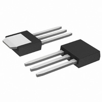
... R TYP I MAX DS(on 8 N−Channel CASE 369AC CASE 369D 3 IPAK DPAK (Straight Lead) (Straight Lead) STYLE 2 MARKING DIAGRAM & PIN ASSIGNMENTS 4 Drain Source Gate Drain Source = Year = Work Week = Pb−Free Package Publication Order Number: NTD60N02R/D ...
Page 2
... Gate Charge SOURCE−DRAIN DIODE CHARACTERISTICS Forward On−Voltage ( Adc Reverse Recovery Time Reverse Recovery Stored Charge 3. Pulse Test: Pulse Width v 300 ms, Duty Cycle v 2%. 4. Switching characteristics are independent of operating junction temperatures. NTD60N02R (T = 25°C unless otherwise noted) J Symbol Vdc Adc) (Note 3) D ...
Page 3
... Figure 3. On−Resistance versus Gate−to−Source Voltage 2 1.8 GS 1.6 1.4 1.2 1.0 0.8 0.6 −50 − JUNCTION TEMPERATURE (°C) J Figure 5. On−Resistance Variation with Temperature NTD60N02R TYPICAL CHARACTERISTICS 120 25° 5.0 V 100 4 175° 2 Figure 2. Transfer Characteristics 0. 25° ...
Page 4
... R , GATE RESISTANCE (W) G Figure 9. Resistive Switching Time Variation versus Gate Resistance 100 V GS SINGLE PULSE 0.1 Figure 11. Maximum Rated Forward Biased Safe Operating Area NTD60N02R 25° iss oss 1 C rss Figure 8. Gate−to−Source and Drain−to−Source Voltage versus Total Charge ...
Page 5
... ORDERING INFORMATION Order Number NTD60N02R NTD60N02RG NTD60N02RT4 NTD60N02RT4G NTD60N02R−1 NTD60N02R−1G NTD60N02R−35 NTD60N02R−35G †For information on tape and reel specifications, including part orientation and tape sizes, please refer to our Tape and Reel Packaging Specifications Brochure, BRD8011/D. NTD60N02R P (pk ...
Page 6
... 0.13 (0.005) M 5.80 0.228 *For additional information on our Pb−Free strategy and soldering details, please download the ON Semiconductor Soldering and Mounting Techniques Reference Manual, SOLDERRM/D. NTD60N02R PACKAGE DIMENSIONS DPAK CASE 369AA−01 ISSUE A SEATING −T− PLANE SOLDERING FOOTPRINT* 6.20 3.0 0.244 ...
Page 7
... SEATING PLANE NTD60N02R PACKAGE DIMENSIONS 3 IPAK, STRAIGHT LEAD CASE 369AC−01 ISSUE 0.13 (0.005) W http://onsemi.com 7 NOTES: 1.. DIMENSIONING AND TOLERANCING PER ANSI Y14.5M, 1982. 2.. CONTROLLING DIMENSION: INCH. 3. SEATING PLANE IS ON TOP OF DAMBAR POSITION. 4. DIMENSION A DOES NOT INCLUDE DAMBAR POSITION OR MOLD GATE. ...
Page 8
... S 0.025 0.040 0.63 1.01 V 0.035 0.050 0.89 1.27 Z 0.155 −−− 3.93 −−− STYLE 2: PIN 1. GATE 2. DRAIN 3. SOURCE 4. DRAIN ON Semiconductor Website: www.onsemi.com Order Literature: http://www.onsemi.com/orderlit For additional information, please contact your local Sales Representative NTD60N02R/D ...