NTY100N10G ON Semiconductor, NTY100N10G Datasheet
NTY100N10G
Specifications of NTY100N10G
Available stocks


Related parts for NTY100N10G

NTY100N10G Summary of contents
Page 1
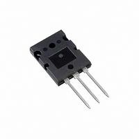
... E 500 0.4 °C/W qJC R 25 Device qJA T 260 °C NTY100N10 L NTY100N10G Preferred devices are recommended choices for future use and best overall value. 1 http://onsemi.com 123 A, 100 (Typ) GS N−Channel MARKING DIAGRAM & PIN ASSIGNMENT NTY100N10 AYYWWG TO−264 STYLE 1 1 ...
Page 2
ELECTRICAL CHARACTERISTICS Characteristic OFF CHARACTERISTICS Drain−Source Breakdown Voltage ( 250 mA (Positive Temperature Coefficient) Zero Gate Voltage Drain Current ( Vdc 100 Vdc 25° ...
Page 3
9 8 150 100 DRAIN−TO−SOURCE VOLTAGE (V) DS Figure 1. On−Region ...
Page 4
Switching behavior is most easily modeled and predicted by recognizing that the power MOSFET is charge controlled. The lengths of various switching intervals (Dt) are determined by how fast the FET input capacitance can be charged by current from the ...
Page 5
100 1000 t d(off 100 ...
Page 6
The Forward Biased Safe Operating Area curves define the maximum simultaneous drain−to−source voltage and drain current that a transistor can handle safely when it is forward biased. Curves are based upon maximum peak junction temperature and a case temperature (T ...
Page 7
D = 0.5 0.2 0.1 0.05 0.1 0.02 0.01 SINGLE PULSE 0.01 1.0E−05 1.0E− Figure 14. Diode Reverse Recovery Waveform SAFE OPERATING AREA P (pk DUTY CYCLE 1.0E−03 1.0E−02 t, ...
Page 8
... American Technical Support: 800−282−9855 Toll Free USA/Canada Japan: ON Semiconductor, Japan Customer Focus Center 2−9−1 Kamimeguro, Meguro−ku, Tokyo, Japan 153−0051 Phone: 81−3−5773−3850 http://onsemi.com 8 NOTES: 1. DIMENSIONING AND TOLERANCING PER ANSI Y14.5M, 1982. 2. CONTROLLING DIMENSION: MILLIMETER. ...