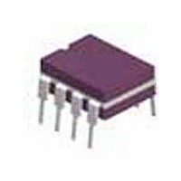
LM193AJ/883 National Semiconductor, LM193AJ/883 Datasheet - Page 3

LM193AJ/883
Manufacturer Part Number
LM193AJ/883
Description
Comparator Dual ±18V/36V 8-Pin CDIP Rail
Manufacturer
National Semiconductor
Specifications of LM193AJ/883
Package
8CDIP
Typical Response Time
1.3 us
Typical Response Time Range
0.5 to 5 us
Typical Voltage Gain Range
90 to 110 dB
Output Type
Open Collector
Number Of Channels Per Chip
2
Minimum Single Supply Voltage
2 V
Power Supply Type
Single|Dual
Number Of Elements
2
Technology
Bipolar
Input Offset Voltage
2mV
Input Bias Current (typ)
1nA
Response Time
1.3us
Single Supply Voltage (typ)
3/5/9/12/15/18/24/28V
Dual Supply Voltage (typ)
±3/±5/±9/±12/±15V
Supply Current (max)
1@5VmA
Power Supply Requirement
Single/Dual
Common Mode Rejection Ratio
60dB
Voltage Gain In Db
106.02dB
Power Supply Rejection Ratio
60dB
Single Supply Voltage (min)
2V
Single Supply Voltage (max)
36V
Dual Supply Voltage (min)
±1V
Dual Supply Voltage (max)
±18V
Power Dissipation
780mW
Operating Temp Range
-55C to 125C
Operating Temperature Classification
Military
Mounting
Through Hole
Pin Count
8
Package Type
CDIP
Lead Free Status / Rohs Status
Not Compliant
Available stocks
Company
Part Number
Manufacturer
Quantity
Price
Company:
Part Number:
LM193AJ/883
Manufacturer:
ZCOMM
Quantity:
1 400
Part Number:
LM193AJ/883
Manufacturer:
NS/国半
Quantity:
20 000
Input Offset Voltage
Input Bias Current
Input Offset Current
Input Common Mode
Voltage Range
Absolute Maximum Ratings
If Military/Aerospace specified devices are required,
please contact the National Semiconductor Sales Office/
Distributors for availability and specifications.
Electrical Characteristics
Electrical Characteristics
(V
Input Offset Voltage
Input Bias Current
Input Offset Current
Input Common Mode
Voltage Range
Supply Current
Voltage Gain
Large Signal Response
Time
Response Time
Output Sink Current
Saturation Voltage
Output Leakage Current
Supply Voltage, V
Differential Input Voltage (Note 8)
Input Voltage
Input Current (V
Power Dissipation (Note 1)
Output Short-Circuit to Ground
Operating Temperature Range
(V
+
Molded DIP
Metal Can
Small Outline Package
micro SMD Pacakge
(Note 2)
LM393
LM293
=5V, T
+
Parameter
=5V, T
Parameter
A
A
= 25˚C, unless otherwise stated)
= 25˚C, unless otherwise stated)
IN
+
<
−0.3V) (Note 3)
(Note 9)
I
Linear Range, V
I
V+ = 30V (Note 6)
IN
IN
(+) or I
(+)−I
IN
(Note 9)
I
Range, V
I
V+ = 30V (Note 6)
R
V
V
V
V
V
V
V
(−) V
IN
IN
IN
R
O
IN
RL
RL
IN
IN
IN
L
(+) or I
(+)−I
(−) with Output In
L
≥15 kΩ, V
(−)=1V, V
(−)=1V, V
(−)=0, V
=TTL Logic Swing, V
=
= 1V to 11V
=5V, R
=5V, R
Conditions
∞
CM
IN
CM
= 0V
(−) V
IN
CM
−25˚C to +85˚C
L
L
−0.3V to +36V
(−) with Output In Linear
= 0V (Note 5)
IN
=5.1 kΩ
=5.1 kΩ (Note 7)
0˚C to +70˚C
+
= 0V (Note 5)
IN
IN
(+)=1V, V
CM
=15V
Continuous
V
V
(+)=0, V
(+)=0, I
(Note 10)
+
+
Conditions
780 mW
660 mW
510 mW
= 0V
=5V
=36V
568mW
50 mA
36V
36V
SINK
O
O
REF
≈1.5V
=5V
≤4 mA
=1.4V
3
Min Typ
0
Storage Temperature Range
Lead Temperature
Soldering Information
See AN-450 “Surface Mounting Methods and Their Effect
on Product Reliability” for other methods of soldering
surface mount devices.
ESD rating
LM193/LM193A
LM2903
(Soldering, 10 seconds)
Dual-In-Line Package
Small Outline Package
(1.5 kΩ in series with 100 pF)
LM193
1.0
3.0
25
Soldering (10 seconds)
Vapor Phase (60 seconds)
Infrared (15 seconds)
V+−1.5
Max
100
5.0
25
Min Typ
LM293, LM393
Min
0
6.0
50
0
1.0
5.0
25
V+−1.5
LM193A
Typ
Max
200
300
250
250
1.0
3.0
0.4
1.3
0.1
5.0
25
16
50
1
Min Typ
0
V
LM2903
Max
+
100
400
2.0
2.5
25
−55˚C to +125˚C
−65˚C to +150˚C
2.0
5.0
−1.5
25
1
−40˚C to +85˚C
V+−1.5
Max
www.national.com
250
7.0
50
+260˚C
1300V
260˚C
215˚C
220˚C
Units
V/mV
mV
mA
mA
mA
mV
nA
nA
nA
ns
µs
V
Units
mV
nA
nA
V


