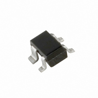
BF1100WR,115 NXP Semiconductors, BF1100WR,115 Datasheet - Page 10

BF1100WR,115
Manufacturer Part Number
BF1100WR,115
Description
MOSFET N-CH 14V 30MA SOT343R
Manufacturer
NXP Semiconductors
Datasheet
1.BF1100WR115.pdf
(16 pages)
Specifications of BF1100WR,115
Package / Case
CMPAK-4
Transistor Type
N-Channel Dual Gate
Frequency
800MHz
Voltage - Rated
14V
Current Rating
30mA
Noise Figure
2dB
Current - Test
10mA
Voltage - Test
9V
Configuration
Single Dual Gate
Transistor Polarity
N-Channel
Drain-source Breakdown Voltage
14 V
Continuous Drain Current
0.03 A
Power Dissipation
280 mW
Maximum Operating Temperature
+ 150 C
Mounting Style
SMD/SMT
Minimum Operating Temperature
- 65 C
Lead Free Status / RoHS Status
Lead free / RoHS Compliant
Power - Output
-
Gain
-
Lead Free Status / RoHS Status
Lead free / RoHS Compliant, Lead free / RoHS Compliant
Other names
934036570115
BF1100WR T/R
BF1100WR T/R
BF1100WR T/R
BF1100WR T/R
NXP Semiconductors
1995 Apr 25
handbook, halfpage
Dual-gate MOS-FET
V
I
V
I
D
D
Fig.24 Forward transfer admittance and phase as
(mS)
DS
DS
(mS)
y fs
= 10 mA; T
= 10 mA; T
y is
10
10
10
= 12 V; V
10
= 12 V; V
10
1
1
2
2
1
10
10
Fig.22 Input admittance as a function of
a function of frequency; typical values.
amb
amb
G2
G2
= 4 V.
= 4 V.
= 25 C.
= 25 C.
frequency; typical values.
10
10
2
2
ϕ
b is
g is
y fs
fs
f (MHz)
f (MHz)
MLD187
MLD185
10
10
3
3
10
10
1
(deg)
ϕ
2
fs
10
handbook, halfpage
V
I
V
I
D
D
Fig.23 Reverse transfer admittance and phase as
(μS)
DS
DS
(mS)
y rs
= 10 mA; T
= 10 mA; T
y os
10
10
10
10
10
= 12 V; V
= 12 V; V
10
1
1
3
2
Fig.25 Output admittance as a function of
1
2
10
10
a function of frequency; typical values.
amb
amb
G2
G2
= 4 V.
= 4 V.
frequency; typical values.
= 25 C.
= 25 C.
10
10
2
ϕ
2
y rs
b os
g os
rs
f (MHz)
f (MHz)
Product specification
BF1100WR
MLD186
MLD188
10
10
3
3
10
10
10
1
(deg)
ϕ
3
rs
2


