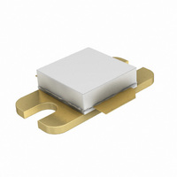
BLS6G3135-20,112 NXP Semiconductors, BLS6G3135-20,112 Datasheet - Page 5

BLS6G3135-20,112
Manufacturer Part Number
BLS6G3135-20,112
Description
TRANS LDMOS 3.5GHZ SOT608A
Manufacturer
NXP Semiconductors
Datasheet
1.BLS6G3135-20112.pdf
(12 pages)
Specifications of BLS6G3135-20,112
Package / Case
SOT-608A
Transistor Type
LDMOS
Frequency
3.1GHz ~ 3.5GHz
Gain
15.5dB
Voltage - Rated
60V
Current Rating
2.1A
Current - Test
50mA
Voltage - Test
32V
Power - Output
20W
Configuration
Single
Transistor Polarity
N-Channel
Resistance Drain-source Rds (on)
0.58 Ohms
Drain-source Breakdown Voltage
60 V
Gate-source Breakdown Voltage
- 0.5 V to + 13 V
Continuous Drain Current
2.1 A
Maximum Operating Temperature
+ 225 C
Mounting Style
SMD/SMT
Minimum Operating Temperature
- 65 C
Application
S-Band
Channel Type
N
Channel Mode
Enhancement
Drain Source Voltage (max)
60V
Output Power (max)
20W(Typ)
Power Gain (typ)@vds
15.5@32VdB
Frequency (min)
3.1GHz
Frequency (max)
3.5GHz
Package Type
CDFM
Pin Count
3
Forward Transconductance (typ)
2.8S
Drain Source Resistance (max)
580mohm
Operating Temp Range
-65C to 225C
Drain Efficiency (typ)
45%
Mounting
Screw
Mode Of Operation
Pulsed RF
Number Of Elements
1
Vswr (max)
5
Screening Level
Military
Lead Free Status / RoHS Status
Lead free / RoHS Compliant
Noise Figure
-
Lead Free Status / Rohs Status
Compliant
Other names
934060062112
BLS6G3135-20
BLS6G3135-20
BLS6G3135-20
BLS6G3135-20
NXP Semiconductors
BLS6G3135-20_6G3135S-20_3
Product data sheet
Fig 2.
Fig 4.
(dB)
(%)
G
(1) f = 3.1 GHz
(2) f = 3.3 GHz
(3) f = 3.5 GHz
D
p
17
15
13
11
60
50
40
30
20
10
9
7
3
0
V
P
Power gain and drain efficiency as functions of
frequency; typical values
V
Efficiency as a function of load power; typical
values
DS
L
DS
= 20 W.
= 32 V; I
= 32 V; I
7.3 Graphs
Dq
Dq
3.2
10
= 50 mA; t
= 50 mA; t
G
p
p
D
p
= 300 s; = 10 %;
= 300 s; = 10 %.
3.4
20
(1)
f (GHz)
P
L
001aaf983
001aaf985
(W)
(2)
(3)
BLS6G3135-20; BLS6G3135S-20
3.6
30
Rev. 03 — 3 March 2009
50
40
30
20
10
0
(%)
D
Fig 3.
Fig 5.
(dB)
(W)
G
P
(1) f = 3.1 GHz
(2) f = 3.3 GHz
(3) f = 3.5 GHz
(1) f = 3.1 GHz
(2) f = 3.3 GHz
(3) f = 3.5 GHz
L
p
17
15
13
11
30
20
10
9
7
0
0
V
Power gain as a function of load power; typical
values
0
V
Load power as a function of input power;
typical values
DS
DS
= 32 V; I
= 32 V; I
LDMOS S-Band radar power transistor
Dq
Dq
0.4
10
= 50 mA; t
= 50 mA; t
p
p
= 300 s; = 10 %.
= 300 s; = 10 %.
(2) (3)
0.8
20
© NXP B.V. 2009. All rights reserved.
P
P
L
i
001aaf984
001aaf986
(W)
(W)
(1)
(2)
(3)
(1)
1.2
30
5 of 12


