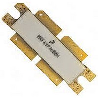
MRF6VP41KHR6 Freescale Semiconductor, MRF6VP41KHR6 Datasheet

MRF6VP41KHR6
Specifications of MRF6VP41KHR6
Related parts for MRF6VP41KHR6
MRF6VP41KHR6 Summary of contents
Page 1
... CASE 375E- -04, STYLE 1 NI- -1230S MRF6VP41KHSR6 PARTS ARE PUSH- -PULL inA GSA outA inB GSB outB (Top View) Figure 1. Pin Connections Symbol Value Unit V --0.5, +110 Vdc DSS V --6, +10 Vdc +150 °C stg T 150 ° 225 ° 1107 W 4.6 W/°C MRF6VP41KHR6 MRF6VP41KHSR6 /V DSA /V DSB 1 ...
Page 2
... MTTF calculator available at http://www.freescale.com/rf. Select Software & Tools/Development Tools/Calculators to access MTTF calculators by product. 2. Refer to AN1955, Thermal Measurement Methodology of RF Power Amplifiers http://www.freescale.com/rf. Select Documentation/Application Notes -- AN1955. 3. Each side of device measured separately. 4. Measurement made with device in push--pull configuration. MRF6VP41KHR6 MRF6VP41KHSR6 2 = 25°C unless otherwise noted) A Symbol I ...
Page 3
... A Symbol G ps η D IRL G ps η D IRL Min Typ Max = 50 Vdc 150 mA 1000 out — 20.1 — — 67 — — --10.2 — Vdc 150 mA 1000 W Peak DD DQ out — 19.5 — — 66 — — --23 — MRF6VP41KHR6 MRF6VP41KHSR6 Unit ...
Page 4
... Z10, Z11 0.316″ x 0.726″ Microstrip Z12, Z13 0.262″ x 0.507″ Microstrip Figure 2. MRF6VP41KHR6(HSR6) Test Circuit Schematic — 450 MHz Table 5. MRF6VP41KHR6(HSR6) Test Circuit Component Designations and Values — 450 MHz Part B1 Ω, 100 MHz Short Ferrite Beads C1, C11 47 μ ...
Page 5
... COAX1 C5 C6 COAX2 L2 B2 C12 C11 Figure 3. MRF6VP41KHR6(HSR6) Test Circuit Component Layout — 450 MHz RF Device Data Freescale Semiconductor C27 MRF6VP41KH Rev C25 L1 C7 C10 C8 C9 C15 C32 C14 C13 C29 C30 C28 C26 COAX3 L3 C22 C23 C18 C19 C16 C17 ...
Page 6
... Vdc 450 MHz 18 150 mA Pulse Width = 100 μsec Duty Cycle = 20 100 P , OUTPUT POWER (WATTS) PULSED out Figure 8. Pulsed Power Gain versus Output Power MRF6VP41KHR6 MRF6VP41KHSR6 6 TYPICAL CHARACTERISTICS 100 Note: Each side of device measured separately η ...
Page 7
... Figure 14. MTTF versus Junction Temperature — --30_C C 85_C 25_C G ps η 100 1000 2000 P , OUTPUT POWER (WATTS) PULSED out versus Output Power 110 130 150 170 190 210 T , JUNCTION TEMPERATURE (° Vdc 1000 W CW, and η = 67%. DD out D MRF6VP41KHR6 MRF6VP41KHSR6 100 230 250 7 ...
Page 8
... Input Matching Network Figure 15. Series Equivalent Source and Load Impedance — 450 MHz MRF6VP41KHR6 MRF6VP41KHSR6 Ω 450 MHz Z source Z load Vdc 150 mA 1000 W Peak DD DQ out source MHz Ω 450 0.86 + j1.06 1.58 + j1. Test circuit impedance as measured from source gate to gate, balanced configuration. ...
Page 9
... C1 C2 COAX2 C10 C12 Figure 16. MRF6VP41KHR6(HSR6) Test Circuit Component Layout — 352.2 MHz Table 6. MRF6VP41KHR6(HSR6) Test Circuit Component Designations and Values — 352.2 MHz Part B1 Ω, 100 MHz Short Ferrite Beads Coax1 Ω Semi Rigid coax, 2.2″ Long C1 Chip Capacitors C3 0 ...
Page 10
... Input Matching Network Figure 17. Series Equivalent Source and Load Impedance — 352.2 MHz MRF6VP41KHR6 MRF6VP41KHSR6 352.2 MHz Z source f = 352.2 MHz Z load Ω Vdc 150 mA 1000 out source MHz Ω 352.2 0.5 + j6.5 2.9 + j6. Test circuit impedance as measured from source gate to gate, balanced configuration. ...
Page 11
... L2 B2 C12 C11 C17 not used in MRF6VP41KHR6(HSR6) 500 MHz application. Figure 18. MRF6VP41KHR6(HSR6) Test Circuit Component Layout — 500 MHz Table 7. MRF6VP41KHR6(HSR6) Test Circuit Component Designations and Values — 500 MHz Part B1 Ω, 100 MHz Short Ferrite Beads Coax1 Ω Semi Rigid coax, 2.2″ Long C1, C11 47 μ ...
Page 12
... Input Matching Network Figure 19. Series Equivalent Source and Load Impedance — 500 MHz MRF6VP41KHR6 MRF6VP41KHSR6 Ω 500 MHz Z load Z source Vdc 150 mA 1000 W Peak DD DQ out source MHz Ω 500 0.75 + j0.5 1.73 + j0. Test circuit impedance as measured from source gate to gate, balanced configuration. ...
Page 13
... RF Device Data Freescale Semiconductor PACKAGE DIMENSIONS MRF6VP41KHR6 MRF6VP41KHSR6 13 ...
Page 14
... MRF6VP41KHR6 MRF6VP41KHSR6 14 RF Device Data Freescale Semiconductor ...
Page 15
... RF Device Data Freescale Semiconductor MRF6VP41KHR6 MRF6VP41KHSR6 15 ...
Page 16
... MRF6VP41KHR6 MRF6VP41KHSR6 16 RF Device Data Freescale Semiconductor ...
Page 17
... MTTF” footnote added • Added Electromigration MTTF Calculator and RF High Power Model availability to Product Software Device Data Freescale Semiconductor REVISION HISTORY Description source MRF6VP41KHR6 MRF6VP41KHSR6 copy to read “Test circuit copy to read “Test circuit load 17 ...
Page 18
... For Literature Requests Only: Freescale Semiconductor Literature Distribution Center 1--800--441--2447 or +1--303--675--2140 Fax: +1--303--675--2150 LDCForFreescaleSemiconductor@hibbertgroup.com MRF6VP41KHR6 MRF6VP41KHSR6 Document Number: MRF6VP41KH Rev. 5, 4/2010 18 Information in this document is provided solely to enable system and software implementers to use Freescale Semiconductor products. There are no express or implied copyright licenses granted hereunder to design or fabricate any integrated circuits or integrated circuits based on the information in this document ...


