BFS17W,115 NXP Semiconductors, BFS17W,115 Datasheet - Page 2
BFS17W,115
Manufacturer Part Number
BFS17W,115
Description
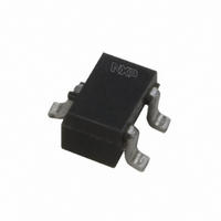
TRANS NPN 15V 1GHZ SOT323
Manufacturer
NXP Semiconductors
Datasheet
1.BFS17W115.pdf
(8 pages)
Specifications of BFS17W,115
Package / Case
SC-70-3, SOT-323-3
Transistor Type
NPN
Voltage - Collector Emitter Breakdown (max)
15V
Frequency - Transition
1.6GHz
Noise Figure (db Typ @ F)
4.5dB @ 500MHz
Power - Max
300mW
Dc Current Gain (hfe) (min) @ Ic, Vce
25 @ 2mA, 1V
Current - Collector (ic) (max)
50mA
Mounting Type
Surface Mount
Dc Current Gain Hfe Max
25 @ 2mA @ 1V
Mounting Style
SMD/SMT
Configuration
Single
Transistor Polarity
NPN
Maximum Operating Frequency
1600 MHz (Typ)
Collector- Emitter Voltage Vceo Max
15 V
Emitter- Base Voltage Vebo
2.5 V
Continuous Collector Current
0.05 A
Power Dissipation
300 mW
Maximum Operating Temperature
+ 175 C
Number Of Elements
1
Collector-emitter Voltage
15V
Collector-base Voltage
25V
Emitter-base Voltage
2.5V
Collector Current (dc) (max)
50mA
Dc Current Gain (min)
25
Frequency (max)
1.6GHz
Operating Temp Range
-65C to 175C
Operating Temperature Classification
Military
Mounting
Surface Mount
Pin Count
3
Package Type
SC-70
Lead Free Status / RoHS Status
Lead free / RoHS Compliant
Gain
-
Lead Free Status / Rohs Status
Lead free / RoHS Compliant
Other names
568-1990-2
934022860115
BFS17W T/R
934022860115
BFS17W T/R


NXP Semiconductors
APPLICATIONS
Primarily intended as a mixer,
oscillator and IF amplifier in UHF and
VHF tuners.
DESCRIPTION
Silicon NPN transistor in a plastic
SOT323 (S-mini) package. The
BFS17W uses the same crystal as
the SOT23 version, BFS17.
QUICK REFERENCE DATA
Note
1. T
LIMITING VALUES
In accordance with the Absolute Maximum Rating System (IEC 134).
Note
1. T
1995 Sep 04
V
V
I
P
h
f
C
C
T
V
V
V
I
P
T
T
C
T
C
SYMBOL
SYMBOL
FE
j
stg
j
CBO
CEO
tot
CBO
CEO
EBO
tot
NPN 1 GHz wideband transistor
c
re
s
s
is the temperature at the soldering point of the collector pin.
is the temperature at the soldering point of the collector pin.
collector-base voltage
collector-emitter voltage
DC collector current
total power dissipation
DC current gain
transition frequency
collector capacitance
feedback capacitance
junction temperature
collector-base voltage
collector-emitter voltage
emitter-base voltage
collector current (DC)
total power dissipation
storage temperature
junction temperature
PARAMETER
PARAMETER
PINNING
up to T
I
I
I
I
open emitter
open base
open collector
T
PIN
C
C
E
C
s
1
2
3
= 0; V
= 2 mA; V
= 25 mA; V
= 1 mA; V
= 118 C; note 1
s
base
emitter
collector
CB
= 118 C; note 1
= 10 V; f = 1 MHz
CONDITIONS
CE
CE
DESCRIPTION
CE
2
= 1 V
= 5 V; f = 1 MHz
CONDITIONS
= 5 V
handbook, 2 columns
25
Marking code: E1
MIN.
Top view
90
1.6
0.8
0.75
65
Fig.1 SOT323
TYP.
MIN.
Product specification
1
25
15
50
300
1.5
175
25
15
2.5
50
300
+150
175
3
MAX.
MAX.
BFS17W
MBC870
2
V
V
mA
mW
GHz
pF
pF
C
V
V
V
mA
mW
C
C
UNIT
UNIT
Related parts for BFS17W,115
Image
Part Number
Description
Manufacturer
Datasheet
Request
R

Part Number:
Description:
TRANS NPN 15V 50MA 1GHZ SOT323
Manufacturer:
NXP Semiconductors
Datasheet:

Part Number:
Description:
NXP Semiconductors designed the LPC2420/2460 microcontroller around a 16-bit/32-bitARM7TDMI-S CPU core with real-time debug interfaces that include both JTAG andembedded trace
Manufacturer:
NXP Semiconductors
Datasheet:

Part Number:
Description:
NXP Semiconductors designed the LPC2458 microcontroller around a 16-bit/32-bitARM7TDMI-S CPU core with real-time debug interfaces that include both JTAG andembedded trace
Manufacturer:
NXP Semiconductors
Datasheet:
Part Number:
Description:
NXP Semiconductors designed the LPC2468 microcontroller around a 16-bit/32-bitARM7TDMI-S CPU core with real-time debug interfaces that include both JTAG andembedded trace
Manufacturer:
NXP Semiconductors
Datasheet:
Part Number:
Description:
NXP Semiconductors designed the LPC2470 microcontroller, powered by theARM7TDMI-S core, to be a highly integrated microcontroller for a wide range ofapplications that require advanced communications and high quality graphic displays
Manufacturer:
NXP Semiconductors
Datasheet:
Part Number:
Description:
NXP Semiconductors designed the LPC2478 microcontroller, powered by theARM7TDMI-S core, to be a highly integrated microcontroller for a wide range ofapplications that require advanced communications and high quality graphic displays
Manufacturer:
NXP Semiconductors
Datasheet:
Part Number:
Description:
The Philips Semiconductors XA (eXtended Architecture) family of 16-bit single-chip microcontrollers is powerful enough to easily handle the requirements of high performance embedded applications, yet inexpensive enough to compete in the market for hi
Manufacturer:
NXP Semiconductors
Datasheet:
Part Number:
Description:
The XA-S3 device is a member of Philips Semiconductors? XA(eXtended Architecture) family of high performance 16-bitsingle-chip microcontrollers
Manufacturer:
NXP Semiconductors
Datasheet:

Part Number:
Description:
The NXP BlueStreak LH75401/LH75411 family consists of two low-cost 16/32-bit System-on-Chip (SoC) devices
Manufacturer:
NXP Semiconductors
Datasheet:
Part Number:
Description:
The NXP LPC3130/3131 combine an 180 MHz ARM926EJ-S CPU core, high-speed USB2
Manufacturer:
NXP Semiconductors
Datasheet:
Part Number:
Description:
The NXP LPC3141 combine a 270 MHz ARM926EJ-S CPU core, High-speed USB 2
Manufacturer:
NXP Semiconductors
Part Number:
Description:
The NXP LPC3143 combine a 270 MHz ARM926EJ-S CPU core, High-speed USB 2
Manufacturer:
NXP Semiconductors

Part Number:
Description:
The NXP LPC3152 combines an 180 MHz ARM926EJ-S CPU core, High-speed USB 2
Manufacturer:
NXP Semiconductors
Part Number:
Description:
The NXP LPC3154 combines an 180 MHz ARM926EJ-S CPU core, High-speed USB 2
Manufacturer:
NXP Semiconductors