BFT92,215 NXP Semiconductors, BFT92,215 Datasheet - Page 4
BFT92,215
Manufacturer Part Number
BFT92,215
Description
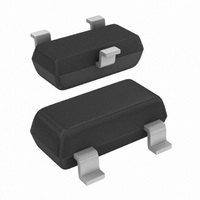
TRANS PNP 25MA 15V 5GHZ SOT23
Manufacturer
NXP Semiconductors
Datasheet
1.BFT92215.pdf
(10 pages)
Specifications of BFT92,215
Package / Case
SOT-23-3, TO-236-3, Micro3™, SSD3, SST3
Transistor Type
PNP
Voltage - Collector Emitter Breakdown (max)
15V
Frequency - Transition
5GHz
Noise Figure (db Typ @ F)
2.5dB @ 500MHz
Power - Max
300mW
Dc Current Gain (hfe) (min) @ Ic, Vce
20 @ 14mA, 10V
Current - Collector (ic) (max)
25mA
Mounting Type
Surface Mount
Dc Collector/base Gain Hfe Min
20 @ 14 mA @ 10 V
Minimum Operating Temperature
- 65 C
Mounting Style
SMD/SMT
Configuration
Single
Transistor Polarity
PNP
Maximum Operating Frequency
5000 MHz (Typ)
Collector- Emitter Voltage Vceo Max
15 V
Emitter- Base Voltage Vebo
2 V
Continuous Collector Current
0.025 A
Power Dissipation
300 mW
Maximum Operating Temperature
+ 175 C
Number Of Elements
1
Collector-emitter Voltage
15V
Collector-base Voltage
20V
Emitter-base Voltage
2V
Collector Current (dc) (max)
25mA
Dc Current Gain (min)
20
Frequency (max)
5GHz
Operating Temp Range
-65C to 175C
Operating Temperature Classification
Military
Mounting
Surface Mount
Pin Count
3
Package Type
TO-236AB
Lead Free Status / RoHS Status
Lead free / RoHS Compliant
Gain
-
Lead Free Status / Rohs Status
Lead free / RoHS Compliant
Other names
568-1655-2
933347730215
BFT92 T/R
933347730215
BFT92 T/R
Available stocks
Company
Part Number
Manufacturer
Quantity
Price
Company:

Part Number:
BFT92,215
Manufacturer:
NXP
Quantity:
36 000


NXP Semiconductors
CHARACTERISTICS
T
Notes
1. G
2. d
November 1992
I
h
f
C
C
G
C
F
V
SYMBOL
j
CBO
T
FE
= 25 C unless otherwise specified.
o
c
e
re
PNP 5 GHz wideband transistor
UM
V
V
V
measured at f
im
G
p
q
r
UM
= V
= V
= V
UM
= 60 dB (DIN 45004B); I
is the maximum unilateral power gain, assuming S
o
o
o
=
6 dB; f
at d
6 dB; f
collector cut-off current
DC current gain
transition frequency
collector capacitance
emitter capacitance
feedback capacitance
maximum unilateral power gain
(note 1)
noise figure
output voltage
10
im
log
(pq-r)
= 60 dB; f
r
q
--------------------------------------------------------- - dB.
= 505.25 MHz;
1
= 503.25 MHz;
–
PARAMETER
= 493.25 MHz.
S
11
S
p
2
1
21
= 495.25 MHz;
C
2
–
= 14 mA; V
S
22
2
CE
note 2
I
I
I
f = 500 MHz
I
I
I
I
f = 500 MHz; T
I
f = 500 MHz; T
= 10 V; R
E
C
C
E
C
C
C
C
= 0; V
= i
= 14 mA; V
= 14 mA; V
= i
= 2 mA; V
= 14 mA; V
= 5 mA; V
e
c
= 0; V
= 0; V
CB
4
12
L
= 10 V;
is zero and
CB
EB
CONDITIONS
= 75 ;
CE
CE
CE
CE
CE
amb
amb
= 0.5 V; f = 1 MHz
= 10 V; f = 1 MHz
= 10 V; f = 1 MHz
= 10 V;
= 10 V
= 10 V;
= 10 V;
= 25 C
= 25 C
20
MIN. TYP. MAX.
50
5
0.75
0.8
0.7
18
2.5
150
Product specification
50
BFT92
nA
GHz
pF
pF
pF
dB
dB
mV
UNIT
Related parts for BFT92,215
Image
Part Number
Description
Manufacturer
Datasheet
Request
R

Part Number:
Description:
NXP Semiconductors designed the LPC2420/2460 microcontroller around a 16-bit/32-bitARM7TDMI-S CPU core with real-time debug interfaces that include both JTAG andembedded trace
Manufacturer:
NXP Semiconductors
Datasheet:

Part Number:
Description:
NXP Semiconductors designed the LPC2458 microcontroller around a 16-bit/32-bitARM7TDMI-S CPU core with real-time debug interfaces that include both JTAG andembedded trace
Manufacturer:
NXP Semiconductors
Datasheet:
Part Number:
Description:
NXP Semiconductors designed the LPC2468 microcontroller around a 16-bit/32-bitARM7TDMI-S CPU core with real-time debug interfaces that include both JTAG andembedded trace
Manufacturer:
NXP Semiconductors
Datasheet:
Part Number:
Description:
NXP Semiconductors designed the LPC2470 microcontroller, powered by theARM7TDMI-S core, to be a highly integrated microcontroller for a wide range ofapplications that require advanced communications and high quality graphic displays
Manufacturer:
NXP Semiconductors
Datasheet:
Part Number:
Description:
NXP Semiconductors designed the LPC2478 microcontroller, powered by theARM7TDMI-S core, to be a highly integrated microcontroller for a wide range ofapplications that require advanced communications and high quality graphic displays
Manufacturer:
NXP Semiconductors
Datasheet:
Part Number:
Description:
The Philips Semiconductors XA (eXtended Architecture) family of 16-bit single-chip microcontrollers is powerful enough to easily handle the requirements of high performance embedded applications, yet inexpensive enough to compete in the market for hi
Manufacturer:
NXP Semiconductors
Datasheet:
Part Number:
Description:
The XA-S3 device is a member of Philips Semiconductors? XA(eXtended Architecture) family of high performance 16-bitsingle-chip microcontrollers
Manufacturer:
NXP Semiconductors
Datasheet:

Part Number:
Description:
The NXP BlueStreak LH75401/LH75411 family consists of two low-cost 16/32-bit System-on-Chip (SoC) devices
Manufacturer:
NXP Semiconductors
Datasheet:
Part Number:
Description:
The NXP LPC3130/3131 combine an 180 MHz ARM926EJ-S CPU core, high-speed USB2
Manufacturer:
NXP Semiconductors
Datasheet:
Part Number:
Description:
The NXP LPC3141 combine a 270 MHz ARM926EJ-S CPU core, High-speed USB 2
Manufacturer:
NXP Semiconductors
Part Number:
Description:
The NXP LPC3143 combine a 270 MHz ARM926EJ-S CPU core, High-speed USB 2
Manufacturer:
NXP Semiconductors

Part Number:
Description:
The NXP LPC3152 combines an 180 MHz ARM926EJ-S CPU core, High-speed USB 2
Manufacturer:
NXP Semiconductors
Part Number:
Description:
The NXP LPC3154 combines an 180 MHz ARM926EJ-S CPU core, High-speed USB 2
Manufacturer:
NXP Semiconductors

Part Number:
Description:
Standard level N-channel enhancement mode Field-Effect Transistor (FET) in a plastic package using NXP High-Performance Automotive (HPA) TrenchMOS technology
Manufacturer:
NXP Semiconductors
Datasheet: