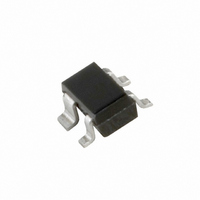
BFG425W,115 NXP Semiconductors, BFG425W,115 Datasheet - Page 9

BFG425W,115
Manufacturer Part Number
BFG425W,115
Description
TRANS NPN 4.5V 25GHZ SOT-343R
Manufacturer
NXP Semiconductors
Datasheet
1.BFG425W115.pdf
(13 pages)
Specifications of BFG425W,115
Package / Case
SOT-343R
Transistor Type
NPN
Voltage - Collector Emitter Breakdown (max)
4.5V
Frequency - Transition
25GHz
Noise Figure (db Typ @ F)
0.8dB ~ 1.2dB @ 900MHz ~ 2GHz
Gain
20dB
Power - Max
135mW
Dc Current Gain (hfe) (min) @ Ic, Vce
50 @ 25mA, 2V
Current - Collector (ic) (max)
30mA
Mounting Type
Surface Mount
Dc Current Gain Hfe Max
50 @ 25mA @ 2V
Mounting Style
SMD/SMT
Configuration
Single Dual Emitter
Transistor Polarity
NPN
Maximum Operating Frequency
25000 MHz (Typ)
Collector- Emitter Voltage Vceo Max
4.5 V
Emitter- Base Voltage Vebo
1 V
Continuous Collector Current
0.03 A
Power Dissipation
135 mW
Maximum Operating Temperature
+ 150 C
Lead Free Status / RoHS Status
Lead free / RoHS Compliant
Lead Free Status / RoHS Status
Lead free / RoHS Compliant, Lead free / RoHS Compliant
Other names
568-1644-2
934047470115
BFG425W T/R
934047470115
BFG425W T/R
Available stocks
Company
Part Number
Manufacturer
Quantity
Price
Part Number:
BFG425W,115
Manufacturer:
NXP/恩智浦
Quantity:
20 000
NXP Semiconductors
SPICE parameters for the BFG425W die
2010 Sep 15
1
2
3
4
5
6
7
8
9
10
11
12
13
14
15
16
17
18
19
20
21
22
23
24
25
26
27
28
29
30
31
32
33
34
35
36
37
38
SEQUENCE No.
NPN 25 GHz wideband transistor
(1)
(1)
(1)
(1)
(1)
(1)
(1)
IS
BF
NF
VAF
IKF
ISE
NE
BR
NR
VAR
IKR
ISC
NC
RB
IRB
RBM
RE
RC
XTB
EG
XTI
CJE
VJE
MJE
TF
XTF
VTF
ITF
PTF
CJC
VJC
MJC
XCJC
TR
CJS
VJS
MJS
FC
PARAMETER VALUE
47.17
145.0
0.993
31.12
304.0
300.2
3.000
11.37
0.985
1.874
0.121
484.8
1.546
14.41
0.000
6.175
177.9
1.780
1.500
1.110
3.000
310.9
900.0
0.346
4.122
68.20
2.004
1.525
0.000
137.7
556.9
0.207
0.500
0.000
667.5
418.3
0.239
0.550
aA
V
mA
fA
V
A
aA
A
m
eV
fF
mV
ps
V
A
deg
fF
mV
ns
fF
mV
UNIT
9
Notes
1. These parameters have not been extracted, the
2. Bonding pad capacity C
3. Bonding pad capacity C
List of components (see Fig.14)
Note
1. External emitter inductance to be added separately
handbook, halfpage
39
40
41
C
C
C
L1
L2
L3 (note 1)
SEQUENCE No.
be
cb
ce
QL
f
(3)
c
(2)(3)
(2)
default values are shown.
resistance R
resistance R
due to the influence of the printed-circuit board.
DESIGNATION
B
= scaling frequency = 1 GHz.
B
Fig.14 Package equivalent circuit SOT343R2.
= 50; QL
C be
L1
E
= 50; QL
sb1
sb2
between B and E.
between C and E.
C
R
R
B,E
PARAMETER VALUE
bp
sb1
sb2
(f) = QL
B'
80
2
80
1.1
1.1
0.25
C cb
bp
bp
E'
E
B,E
VALUE
L3
in series with substrate
in series with substrate
C'
(f/f
c
)
Product specification
145
25
19
BFG425W
fF
fF
fF
nH
nH
nH
C
MGD956
L2
ce
UNIT
fF
UNIT
C


