ST333C04CFL0 Vishay, ST333C04CFL0 Datasheet - Page 2
ST333C04CFL0
Manufacturer Part Number
ST333C04CFL0
Description
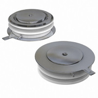
SCR PHASE CONT 400V 720A E-PUK
Manufacturer
Vishay
Specifications of ST333C04CFL0
Scr Type
Standard Recovery
Voltage - Off State
400V
Voltage - Gate Trigger (vgt) (max)
3V
Voltage - On State (vtm) (max)
1.96V
Current - On State (it (av)) (max)
720A
Current - On State (it (rms)) (max)
1435A
Current - Gate Trigger (igt) (max)
200mA
Current - Hold (ih) (max)
600mA
Current - Off State (max)
50mA
Current - Non Rep. Surge 50, 60hz (itsm)
11000A, 11500A
Operating Temperature
-40°C ~ 125°C
Mounting Type
Chassis Mount
Package / Case
TO-200AB, E-PUK
Current - On State (it (rms) (max)
1435A
Breakover Current Ibo Max
11500 A
Rated Repetitive Off-state Voltage Vdrm
400 V
Off-state Leakage Current @ Vdrm Idrm
50 mA
Forward Voltage Drop
1.96 V
Gate Trigger Voltage (vgt)
3 V
Maximum Gate Peak Inverse Voltage
5 V
Gate Trigger Current (igt)
200 mA
Holding Current (ih Max)
600 mA
Mounting Style
SMD/SMT
Peak Repetitive Off-state Voltage, Vdrm
400V
Gate Trigger Current Max, Igt
200mA
Current It Av
720A
On State Rms Current It(rms)
1.435kA
Peak Non Rep Surge Current Itsm 50hz
11kA
Lead Free Status / RoHS Status
Lead free / RoHS Compliant
Other names
*ST333C04CFL0
VS-ST333C04CFL0
VS-ST333C04CFL0
VSST333C04CFL0
VSST333C04CFL0
VS-ST333C04CFL0
VS-ST333C04CFL0
VSST333C04CFL0
VSST333C04CFL0


ST333C..C Series
Vishay High Power Products
www.vishay.com
2
CURRENT CARRYING CAPABILITY
FREQUENCY
50 Hz
400 Hz
1000 Hz
2500 Hz
Recovery voltage V
Voltage before turn-on V
Rise of on-state current dI/dt
Heatsink temperature
Equivalent values for RC circuit
ON-STATE CONDUCTION
PARAMETER
Maximum average on-state current
at heatsink temperature
Maximum RMS on-state current
Maximum peak, one half cycle,
non-repetitive surge current
Maximum I
Maximum I
Maximum peak on-state voltage
Low level value of threshold voltage
High level value of threshold voltage
Low level value of forward slope resistance
High level value of forward slope resistance
Maximum holding current
Typical latching current
SWITCHING
PARAMETER
Maximum non-repetitive rate of rise
of turned on current
Typical delay time
Maximum turn-off time
2
2
t for fusing
√t for fusing
r
d
For technical questions, contact: ind-modules@vishay.com
1630
1630
1350
720
40
SYMBOL
SYMBOL
180° el
V
V
I
dI/dt
I
T(RMS)
I
T(AV)
V
T(TO)1
T(TO)2
(Hockey PUK Version), 720 A
t
t
TSM
10/0.47
I
I
r
r
I
d
q
I
2
2
TM
t1
t2
H
L
V
t
√t
Inverter Grade Thyristors
50
DRM
50
1420
1390
1090
550
T
T
Resistive load, gate pulse: 10 V, 5 Ω source
T
I
V
55
TM
I
J
J
J
TM
180° conduction, half sine wave
Double side (single side) cooled
DC at 25 °C heatsink temperature double side cooled
t = 10 ms
t = 8.3 ms
t = 10 ms
t = 8.3 ms
t = 10 ms
t = 8.3 ms
t = 10 ms
t = 8.3 ms
t = 0.1 to 10 ms, no voltage reapplied
I
(16.7 % x π x I
(I > π x I
(16.7 % x π x I
(I > π x I
T
T
R
TM
= T
= 25 °C, V
= T
J
J
= 50 V, t
= 550 A, commutating dI/dt = 40 A/µs
= 25 °C, I
= 25 °C, V
= 1810 A, T
J
J
maximum, V
maximum,
T(AV)
T(AV)
p
DM
= 500 µs, dV/dt: See table in device code
2520
2670
2440
1450
T
), T
), T
A
40
> 30 A
T(AV)
T(AV)
J
= Rated V
No voltage
reapplied
100 % V
reapplied
No voltage
reapplied
100 % V
reapplied
= 12 V, R
TEST CONDITIONS
J
J
= T
180° el
= T
= T
TEST CONDITIONS
10/0.47
DRM
V
J
< I < π x I
< I < π x I
50
maximum, t
DRM
J
J
-
maximum
maximum
= Rated V
RRM
RRM
a
DRM
= 6 Ω, I
2260
2330
2120
1220
I
55
TM
T(AV)
T(AV)
, I
Sinusoidal half wave,
initial T
TM
p
), T
), T
DRM
G
= 10 ms sine wave pulse
= 50 A DC, t
= 1 A
J
J
; I
J
= T
= T
TM
= T
7610
4080
2420
1230
J
J
= 2 x dI/dt
40
J
maximum
maximum
maximum
100 µs
p
10/0.47
= 1 µs
V
50
DRM
-
Document Number: 93678
6820
3600
2100
1027
I
55
TM
MIN. MAX.
10
VALUES
Revision: 15-May-08
720 (350)
VALUES
1000
55 (75)
11 000
11 500
1.1
1435
9250
9700
6050
1000
1.96
0.91
0.93
0.58
0.58
605
553
428
391
600
30
UNITS
Ω/µF
A/µs
°C
UNITS
A
V
UNITS
kA
kA
mΩ
A/µs
mA
°C
A
A
V
µs
2
2
s
√s
Related parts for ST333C04CFL0
Image
Part Number
Description
Manufacturer
Datasheet
Request
R

Part Number:
Description:
357-036-542-201 CARDEDGE 36POS DL .156 BLK LOPRO
Manufacturer:
Vishay
Datasheet:
Part Number:
Description:
357-036-542-201 CARDEDGE 36POS DL .156 BLK LOPRO
Manufacturer:
Vishay
Datasheet:
Part Number:
Description:
357-036-542-201 CARDEDGE 36POS DL .156 BLK LOPRO
Manufacturer:
Vishay
Datasheet:
Part Number:
Description:
357-036-542-201 CARDEDGE 36POS DL .156 BLK LOPRO
Manufacturer:
Vishay
Datasheet:
Part Number:
Description:
357-036-542-201 CARDEDGE 36POS DL .156 BLK LOPRO
Manufacturer:
Vishay
Datasheet:
Part Number:
Description:
357-036-542-201 CARDEDGE 36POS DL .156 BLK LOPRO
Manufacturer:
Vishay
Datasheet:
Part Number:
Description:
357-036-542-201 CARDEDGE 36POS DL .156 BLK LOPRO
Manufacturer:
Vishay
Datasheet:
Part Number:
Description:
357-036-542-201 CARDEDGE 36POS DL .156 BLK LOPRO
Manufacturer:
Vishay
Datasheet:
Part Number:
Description:
357-036-542-201 CARDEDGE 36POS DL .156 BLK LOPRO
Manufacturer:
Vishay
Datasheet:
Part Number:
Description:
357-036-542-201 CARDEDGE 36POS DL .156 BLK LOPRO
Manufacturer:
Vishay
Datasheet:
Part Number:
Description:
357-036-542-201 CARDEDGE 36POS DL .156 BLK LOPRO
Manufacturer:
Vishay
Datasheet:
Part Number:
Description:
357-036-542-201 CARDEDGE 36POS DL .156 BLK LOPRO
Manufacturer:
Vishay
Datasheet:
Part Number:
Description:
357-036-542-201 CARDEDGE 36POS DL .156 BLK LOPRO
Manufacturer:
Vishay
Datasheet:
Part Number:
Description:
357-036-542-201 CARDEDGE 36POS DL .156 BLK LOPRO
Manufacturer:
Vishay
Datasheet:
Part Number:
Description:
357-036-542-201 CARDEDGE 36POS DL .156 BLK LOPRO
Manufacturer:
Vishay
Datasheet: