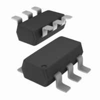
PBSS4240DPN,115 NXP Semiconductors, PBSS4240DPN,115 Datasheet - Page 3

PBSS4240DPN,115
Manufacturer Part Number
PBSS4240DPN,115
Description
TRANS NPN/PNP 40V 1.35A SC-74
Manufacturer
NXP Semiconductors
Datasheet
1.PBSS4240DPN115.pdf
(12 pages)
Specifications of PBSS4240DPN,115
Package / Case
SC-74-6
Transistor Type
NPN, PNP
Current - Collector (ic) (max)
1.35A, 1.1A
Voltage - Collector Emitter Breakdown (max)
40V
Vce Saturation (max) @ Ib, Ic
400mV @ 200mA, 2A / 530mV @ 200mA, 2A
Current - Collector Cutoff (max)
100nA
Dc Current Gain (hfe) (min) @ Ic, Vce
300 @ 500mA, 5V / 300 @ 100mA, 5V
Power - Max
1.1W
Frequency - Transition
150MHz
Mounting Type
Surface Mount
Dc Collector/base Gain Hfe Min
50
Minimum Operating Temperature
- 65
Configuration
Dual
Transistor Polarity
NPN/PNP
Mounting Style
SMD/SMT
Collector- Emitter Voltage Vceo Max
+/- 40 V
Emitter- Base Voltage Vebo
5 V
Continuous Collector Current
1.35 A, - 1.1 A
Maximum Dc Collector Current
+/- 3 A
Power Dissipation
370 mW
Maximum Operating Frequency
150 MHz
Maximum Operating Temperature
+ 150 C
Lead Free Status / RoHS Status
Lead free / RoHS Compliant
Lead Free Status / RoHS Status
Lead free / RoHS Compliant, Lead free / RoHS Compliant
Other names
568-4349-2
934057314115
PBSS4240DPN T/R
PBSS4240DPN T/R
934057314115
PBSS4240DPN T/R
PBSS4240DPN T/R
NXP Semiconductors
LIMITING VALUES
In accordance with the Absolute Maximum Rating System (IEC 60134).
Notes
1. Operated under pulsed conditions: duty cycle δ ≤ 20%; pulse width tp ≤ 10 ms; mounting pad for collector standard
2. Device mounted on a printed-circuit board; single-sided copper; tinplated; mounting pad for collector 1 cm
3. Device mounted on a printed-circuit board; single-sided copper; tinplated; standard footprint.
THERMAL CHARACTERISTICS
Notes
1. Device mounted on a printed-circuit board, single-sided copper, tinplated, mounting pad for collector 1 cm
2. Operated under pulsed conditions: pulse width t
2003 Feb 20
Per transistor unless otherwise specified; for the PNP transistor with negative polarity
V
V
V
I
I
I
I
I
P
T
T
T
Per device
P
Per transistor
R
SYMBOL
SYMBOL
C
CRP
CM
B
BM
stg
j
amb
CBO
CEO
EBO
tot
tot
40 V low V
th j-a
footprint.
footprint.
collector-base voltage
collector-emitter voltage
emitter-base voltage
collector current (DC)
repetitive peak collector current
peak collector current
base current (DC)
peak base current
total power dissipation
storage temperature
junction temperature
operating ambient temperature
total power dissipation
thermal resistance from junction to
ambient
NPN
PNP
CEsat
PARAMETER
PARAMETER
NPN/PNP transistor
open emitter
open base
open collector
note 1
single peak
T
T
T
T
in free air; note 1
in free air; note 2
p
amb
amb
amb
amb
≤ 10 ms; duty cycle δ ≤ 0.20; mounting pad for collector standard
≤ 25 °C; note 2
≤ 25 °C; note 3
≤ 25 °C; note 1
≤ 25 °C; note 2
3
CONDITIONS
CONDITIONS
−
−
−
−
−
−
−
−
−
−
−
−
−
−65
−
−65
−
MIN.
VALUE
340
110
PBSS4240DPN
40
40
5
1.35
−1.1
2
3
300
1
370
310
1.1
+150
150
+150
600
MAX.
Product data sheet
UNIT
K/W
K/W
V
V
V
A
A
A
A
mA
A
mW
mW
W
°C
°C
°C
mW
2
2
.
.
UNIT


