PEMZ1,115 NXP Semiconductors, PEMZ1,115 Datasheet - Page 2
PEMZ1,115
Manufacturer Part Number
PEMZ1,115
Description
TRANS NPN/PNP 40V 100MA SOT666
Manufacturer
NXP Semiconductors
Datasheet
1.PEMZ1115.pdf
(7 pages)
Specifications of PEMZ1,115
Package / Case
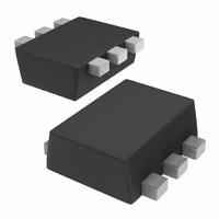
SS Mini-6 (SOT-666)
Transistor Type
NPN, PNP
Current - Collector (ic) (max)
100mA
Voltage - Collector Emitter Breakdown (max)
40V
Vce Saturation (max) @ Ib, Ic
200mV @ 5mA, 50mA
Dc Current Gain (hfe) (min) @ Ic, Vce
120 @ 1mA, 6V
Power - Max
300mW
Frequency - Transition
100MHz
Mounting Type
Surface Mount
Dc Collector/base Gain Hfe Min
120
Minimum Operating Temperature
- 65 C
Configuration
Dual
Transistor Polarity
NPN/PNP
Mounting Style
SMD/SMT
Collector- Emitter Voltage Vceo Max
40 V
Emitter- Base Voltage Vebo
5 V
Continuous Collector Current
100 mA
Maximum Dc Collector Current
200 mA
Power Dissipation
200 mW
Maximum Operating Frequency
100 MHz
Maximum Operating Temperature
+ 150 C
Lead Free Status / RoHS Status
Lead free / RoHS Compliant
Current - Collector Cutoff (max)
-
Lead Free Status / Rohs Status
Lead free / RoHS Compliant
Other names
934056705115
PEMZ1 T/R
PEMZ1 T/R
PEMZ1 T/R
PEMZ1 T/R


NXP Semiconductors
FEATURES
• 300 mW total power dissipation
• Very small 1.6 × 1.2 mm ultra thin package
• Self alignment during soldering due to straight leads
• Replaces two SC-75/SC-89 packaged transistors on
• Reduced required PCB area
• Reduced pick and place costs.
APPLICATIONS
• General purpose switching and amplification
• Complementary MOSFET driver for switch mode power
• Complementary driver for audio amplifiers.
DESCRIPTION
NPN/PNP transistor pair in a SOT666 plastic package.
MARKING
LIMITING VALUES
In accordance with the Absolute Maximum Rating System (IEC 60134).
Note
1. Transistor mounted on an FR4 printed-circuit board.
2001 Nov 07
PEMZ1
Per transistor; for the PNP transistor with negative polarity
V
V
V
I
I
I
P
T
T
T
Per device
P
SYMBOL
C
CM
BM
same PCB area
supply
stg
j
amb
CBO
CEO
EBO
tot
tot
NPN/PNP general purpose transistors
TYPE NUMBER
collector-base voltage
collector-emitter voltage
emitter-base voltage
collector current (DC)
peak collector current
peak base current
total power dissipation
storage temperature
junction temperature
operating ambient temperature
total power dissipation
PARAMETER
MARKING CODE
FZ
open emitter
open base
open collector
T
T
amb
amb
≤ 25 °C; note 1
≤ 25 °C; note 1
2
CONDITIONS
PINNING
handbook, halfpage
Top view
PIN
1, 4
2, 5
6, 3
Fig.1 Simplified outline (SOT666) and symbol.
6
1
emitter
base
collector
5
2
3
4
−
−
−
−
−
−
−
−65
−
−65
−
TR1; TR2
TR1; TR2
TR1; TR2
MIN.
DESCRIPTION
MAM456
TR1
50
40
5
100
200
200
200
+150
150
+150
300
Product data sheet
MAX.
6
1
5
2
PEMZ1
V
V
V
mA
mA
mA
mW
°C
°C
°C
mW
4
3
TR2
UNIT
Related parts for PEMZ1,115
Image
Part Number
Description
Manufacturer
Datasheet
Request
R

Part Number:
Description:
Npn/pnp General Purpose Transistors
Manufacturer:
NXP Semiconductors
Datasheet:
Part Number:
Description:
Transistors Bipolar - BJT TRANS DOUBLE TAPE-7
Manufacturer:
NXP Semiconductors
Datasheet:
Part Number:
Description:
NXP Semiconductors designed the LPC2420/2460 microcontroller around a 16-bit/32-bitARM7TDMI-S CPU core with real-time debug interfaces that include both JTAG andembedded trace
Manufacturer:
NXP Semiconductors
Datasheet:

Part Number:
Description:
NXP Semiconductors designed the LPC2458 microcontroller around a 16-bit/32-bitARM7TDMI-S CPU core with real-time debug interfaces that include both JTAG andembedded trace
Manufacturer:
NXP Semiconductors
Datasheet:
Part Number:
Description:
NXP Semiconductors designed the LPC2468 microcontroller around a 16-bit/32-bitARM7TDMI-S CPU core with real-time debug interfaces that include both JTAG andembedded trace
Manufacturer:
NXP Semiconductors
Datasheet:
Part Number:
Description:
NXP Semiconductors designed the LPC2470 microcontroller, powered by theARM7TDMI-S core, to be a highly integrated microcontroller for a wide range ofapplications that require advanced communications and high quality graphic displays
Manufacturer:
NXP Semiconductors
Datasheet:
Part Number:
Description:
NXP Semiconductors designed the LPC2478 microcontroller, powered by theARM7TDMI-S core, to be a highly integrated microcontroller for a wide range ofapplications that require advanced communications and high quality graphic displays
Manufacturer:
NXP Semiconductors
Datasheet:
Part Number:
Description:
The Philips Semiconductors XA (eXtended Architecture) family of 16-bit single-chip microcontrollers is powerful enough to easily handle the requirements of high performance embedded applications, yet inexpensive enough to compete in the market for hi
Manufacturer:
NXP Semiconductors
Datasheet:
Part Number:
Description:
The XA-S3 device is a member of Philips Semiconductors? XA(eXtended Architecture) family of high performance 16-bitsingle-chip microcontrollers
Manufacturer:
NXP Semiconductors
Datasheet:

Part Number:
Description:
The NXP BlueStreak LH75401/LH75411 family consists of two low-cost 16/32-bit System-on-Chip (SoC) devices
Manufacturer:
NXP Semiconductors
Datasheet:
Part Number:
Description:
The NXP LPC3130/3131 combine an 180 MHz ARM926EJ-S CPU core, high-speed USB2
Manufacturer:
NXP Semiconductors
Datasheet:
Part Number:
Description:
The NXP LPC3141 combine a 270 MHz ARM926EJ-S CPU core, High-speed USB 2
Manufacturer:
NXP Semiconductors
Part Number:
Description:
The NXP LPC3143 combine a 270 MHz ARM926EJ-S CPU core, High-speed USB 2
Manufacturer:
NXP Semiconductors

Part Number:
Description:
The NXP LPC3152 combines an 180 MHz ARM926EJ-S CPU core, High-speed USB 2
Manufacturer:
NXP Semiconductors