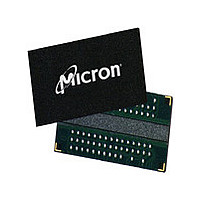
MT47H32M16HR-3 IT:F TR Micron Technology Inc, MT47H32M16HR-3 IT:F TR Datasheet - Page 122

MT47H32M16HR-3 IT:F TR
Manufacturer Part Number
MT47H32M16HR-3 IT:F TR
Description
DRAM Chip DDR2 SDRAM 512M-Bit 32Mx16 1.8V 84-Pin FBGA T/R
Manufacturer
Micron Technology Inc
Type
DDR2 SDRAMr
Specifications of MT47H32M16HR-3 IT:F TR
Density
512 Mb
Maximum Clock Rate
667 MHz
Package
84FBGA
Address Bus Width
15 Bit
Operating Supply Voltage
1.8 V
Maximum Random Access Time
0.45 ns
Operating Temperature
-40 to 85 °C
Organization
32Mx16
Address Bus
15b
Access Time (max)
450ps
Operating Supply Voltage (typ)
1.8V
Package Type
FBGA
Operating Temp Range
-40C to 85C
Operating Supply Voltage (max)
1.9V
Operating Supply Voltage (min)
1.7V
Supply Current
250mA
Pin Count
84
Mounting
Surface Mount
Operating Temperature Classification
Industrial
Lead Free Status / RoHS Status
Compliant
- Current page: 122 of 132
- Download datasheet (10Mb)
Figure 75: PRECHARGE Command-to-Power-Down Entry
Figure 76: LOAD MODE Command-to-Power-Down Entry
PDF: 09005aef82f1e6e2
512MbDDR2.pdf - Rev. R 12/10 EN
Notes:
Note:
Command
Command
Address
Address
1. The earliest precharge power-down entry may occur is at T2, which is 1 ×
1. Valid address for LM command includes MR, EMR, EMR(2), and EMR(3) registers.
2. All banks must be in the precharged state and
3. The earliest precharge power-down entry is at T3, which is after
CK#
CKE
CK#
A10
CKE
CK
PRECHARGE command. Precharge power-down entry occurs prior to
isfied.
CK
Valid
T0
Valid
T0
t RP 2
Valid 1
LM
T1
Single bank
Valid
All banks
122
PRE
T1
vs
1 x
t MRD
t
CK
NOP
Micron Technology, Inc. reserves the right to change products or specifications without notice.
T2
Power-down 1
512Mb: x4, x8, x16 DDR2 SDRAM
entry
NOP
T2
t
Power-down 3
RP met prior to issuing LM command.
entry
NOP
T3
t
CKE (MIN)
T3
Power-Down Mode
© 2004 Micron Technology, Inc. All rights reserved.
t CKE (MIN)
Don’t Care
t
MRD is satisfied.
T4
t
RP (MIN) being sat-
Don’t Care
t
CK after the
Related parts for MT47H32M16HR-3 IT:F TR
Image
Part Number
Description
Manufacturer
Datasheet
Request
R

Part Number:
Description:
IC DDR2 SDRAM 512MBIT 84FBGA
Manufacturer:
Micron Technology Inc
Datasheet:

Part Number:
Description:
IC DDR2 SDRAM 512MBIT 3NS 84FBGA
Manufacturer:
Micron Technology Inc
Datasheet:

Part Number:
Description:
32MX16 DDR2 SDRAM PLASTIC IND TEMP PBF FBGA 1.8V
Manufacturer:
Micron Technology Inc
Datasheet:

Part Number:
Description:
Manufacturer:
Micron Technology Inc
Datasheet:

Part Number:
Description:
Manufacturer:
Micron Technology Inc
Datasheet:

Part Number:
Description:
Manufacturer:
Micron Technology Inc
Datasheet:

Part Number:
Description:
Manufacturer:
Micron Technology Inc
Datasheet:

Part Number:
Description:
MICMT47H32M16HR-3_IT:F 32MBX16 DDR2
Manufacturer:
Micron Technology Inc
Datasheet:

Part Number:
Description:
Manufacturer:
Micron Technology Inc
Datasheet:

Part Number:
Description:
Manufacturer:
Micron Technology Inc
Datasheet:

Part Number:
Description:
Manufacturer:
Micron Technology Inc
Datasheet:

Part Number:
Description:
32MX16 DDR2 SDRAM PLASTIC IND TEMP PBF FBGA 1.8V
Manufacturer:
Micron Technology Inc

Part Number:
Description:
IC DDR2 SDRAM 512MBIT 84FBGA
Manufacturer:
Micron Technology Inc
Datasheet:

Part Number:
Description:
Manufacturer:
Micron Technology Inc
Datasheet:

Part Number:
Description:
Manufacturer:
Micron Technology Inc
Datasheet:


