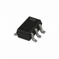
PUMB30,115 NXP Semiconductors, PUMB30,115 Datasheet - Page 8

PUMB30,115
Manufacturer Part Number
PUMB30,115
Description
TRANS PNP/PNP W/RES 50V SOT-363
Manufacturer
NXP Semiconductors
Datasheet
1.PUMB30115.pdf
(10 pages)
Specifications of PUMB30,115
Package / Case
SC-70-6, SC-88, SOT-363
Transistor Type
2 PNP - Pre-Biased (Dual)
Current - Collector (ic) (max)
100mA
Voltage - Collector Emitter Breakdown (max)
50V
Resistor - Base (r1) (ohms)
2.2K
Dc Current Gain (hfe) (min) @ Ic, Vce
30 @ 20mA, 5V
Vce Saturation (max) @ Ib, Ic
150mV @ 500µA, 10mA
Current - Collector Cutoff (max)
1µA
Power - Max
300mW
Mounting Type
Surface Mount
Configuration
Dual
Transistor Polarity
PNP
Typical Input Resistor
2.2 KOhm
Mounting Style
SMD/SMT
Collector- Emitter Voltage Vceo Max
50 V
Peak Dc Collector Current
100 mA
Maximum Operating Temperature
+ 150 C
Minimum Operating Temperature
- 65 C
Lead Free Status / RoHS Status
Lead free / RoHS Compliant
Frequency - Transition
-
Resistor - Emitter Base (r2) (ohms)
-
Lead Free Status / RoHS Status
Lead free / RoHS Compliant, Lead free / RoHS Compliant
Other names
934059933115
PUMB30 T/R
PUMB30 T/R
PUMB30 T/R
PUMB30 T/R
NXP Semiconductors
11. Revision history
Table 10.
PEMB30_PUMB30_2
Product data sheet
Document ID
PEMB30_PUMB30_2
Modifications:
PEMB30_PUMB30_1
Revision history
Release date
20090902
20060331
•
•
•
•
•
This data sheet was changed to reflect the new company name NXP Semiconductors,
including new legal definitions and disclaimers. No changes were made to the technical
content.
Figure 3 “Package outline SOT363 (SC-88)”
Figure 5 “Reflow soldering footprint SOT363
Figure 6 “Wave soldering footprint SOT363
Figure 7 “Reflow soldering footprint
PNP/PNP double resistor-equipped transistors; R1 = 2.2 k , R2 = open
Data sheet status
Product data sheet
Product data sheet
Rev. 02 — 2 September 2009
SOT666”: updated
(SC-88)”: updated
: updated
Change notice
-
-
(SC-88)”: updated
PEMB30; PUMB30
Supersedes
PEMB30_PUMB30_1
-
© NXP B.V. 2009. All rights reserved.
8 of 10


