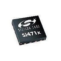
Si4711-A20-GM Silicon Laboratories Inc, Si4711-A20-GM Datasheet - Page 20

Si4711-A20-GM
Manufacturer Part Number
Si4711-A20-GM
Description
RF Transmitter Broadcast FM Radio Trns w/RDS/RBDS
Manufacturer
Silicon Laboratories Inc
Datasheet
1.SI4711-A20-GM.pdf
(38 pages)
Specifications of Si4711-A20-GM
Lead Free Status / RoHS Status
Lead free / RoHS Compliant
Si4710/11-A20
supports a number of industry-standard sampling rates
including 32, 40, 44.1, and 48 kHz. The digital audio
interface enables low-power operation by eliminating
the need for redundant DACs and ADCs on the audio
baseband processor.
The Si4710/11 includes a low-noise stereo line input
(LIN/RIN) with programmable attenuation. To ensure
optimal audio performance, the Si4710/11 has a
transmit line input property that allows the user to
specify the peak amplitude of the analog input required
to reach maximum deviation level. The deviation levels
of the audio, pilot, and RDS/RBDS signals can be
independently programmed to customize FM transmitter
designs. The Si4710/11 has a programmable low audio
level and high audio level indicators that allows the user
to selectively enable and disable the carrier based on
the presence of audio content. In addition, the device
provides an overmodulation indicator to allow the user
to dynamically set the maximum deviation level. The
Si4710/11 has a programmable audio dynamic range
control that can be used to reduce the dynamic range of
the audio input signal and increase the volume at the
receiver. These features can dramatically improve the
end user’s listening experience.
The Si4710/11 is reset by applying a logic low on the
RST pin. This causes all register values to be reset to
their default values. The digital input/output interface
supply (V
RCLK, DIN, DFS, and DCLK pins and can be connected
to the audio baseband processor's supply voltage to
save power and remove the need for voltage level
translators. RCLK is not required for register operation.
The Si4710/11 reference clock is programmable,
supporting many RCLK inputs as shown in Table 9.
5.2. FM Transmitter
The Si4710/11 transmitter uses a digital architecture.
The transmitter (TX) integrates a stereo 16-bit audio
ADC to convert analog audio signals to high fidelity
digital signals. Alternatively, digital audio signals can be
applied to the Si4710/11 directly to reduce power
consumption by eliminating the need to convert audio
baseband signals to analog and back again to digital.
Digital signal processing is used to perform the stereo
MPX encoding and FM modulation to a low digital IF.
Transmit baseband filters suppress out-of-channel
noise and images from the digital low-IF signal. A
quadrature single-sideband mixer up-converts the
digital IF signal to RF, and internal RF filters suppress
noise and harmonics to support the harmonic emission
requirements of cellular phones, GPS, WLAN, and other
wireless standards.
The TXO output has over 10 dB of output level control,
20
IO
) provides voltage to the RST, SEN, SDIO,
Rev. 1.1
programmable in approximately 1 dB steps. This large
output range enables a variety of antennas to be used
for transmit, such as a monopole stub antenna or a loop
antenna. The 1 dB step size provides fine adjustment of
the output voltage.
The TXO output requires only one external 120 nH
inductor. The inductor is used to resonate the antenna
and is automatically calibrated within the integrated
circuit to provide the optimum output level and
frequency response for supported transmit frequencies.
Users are responsible for adjusting their system’s
radiated power levels to comply with local regulations
on RF transmission (FCC, ETSI, ARIB, etc.).
5.3. Digital Audio Interface
The digital audio interface operates in slave mode and
supports 3 different audio data formats:
1. I
2. Left-Justified
3. DSP Mode
5.3.1. Audio Data Formats
In I
edge of DCLK following each DFS transition. The
remaining bits of the word are sent in order, down to the
LSB. The Left Channel is transferred first when the DFS
is low, and the Right Channel is transferred when the
DFS is high.
In Left-Justified mode, the MSB is captured on the first
rising edge of DCLK following each DFS transition. The
remaining bits of the word are sent in order, down to the
LSB. The Left Channel is transferred first when the DFS
is high, and the Right Channel is transferred when the
DFS is low.
In DSP mode, the DFS becomes a pulse with a width of
1DCLK period. The Left Channel is transferred first,
followed right away by the Right Channel. There are two
options in transferring the digital audio data in DSP
mode: the MSB of the left channel can be transferred on
the first rising edge of DCLK following the DFS pulse or
on the second rising edge.
In all audio formats, depending on the word size, DCLK
frequency and sample rates, there may be unused
DCLK cycles after the LSB of each word before the next
DFS transition and MSB of the next word.
The number of audio bits can be configured for 8, 16,
20, or 24 bits.
2
2
S mode, the MSB is captured on the second rising
S


