PXT2222A,115 NXP Semiconductors, PXT2222A,115 Datasheet
PXT2222A,115
Specifications of PXT2222A,115
933821820115
PXT2222A T/R
Available stocks


Related parts for PXT2222A,115


PXT2222A,115 Summary of contents
Page 1
DATA SHEET dbook, halfpage PXT2222A NPN switching transistor Product data sheet Supersedes data of 1999 Apr 14 DISCRETE SEMICONDUCTORS M3D109 2004 Nov 22 ...
Page 2
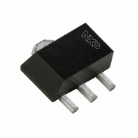
... NXP Semiconductors NPN switching transistor FEATURES • High current (max. 600 mA) • Low voltage (max. 40 V). APPLICATIONS • General purpose switching and linear amplification. DESCRIPTION NPN switching transistor in a SOT89 plastic package. PNP complement: PXT2907A. MARKING TYPE NUMBER PXT2222A *1P Note Made in Hong Kong. ...
Page 3
... NXP Semiconductors NPN switching transistor LIMITING VALUES In accordance with the Absolute Maximum Rating System (IEC 60134). SYMBOL PARAMETER V collector-base voltage CBO V collector-emitter voltage CEO V emitter-base voltage EBO I collector current (DC peak collector current CM I peak base current BM P total power dissipation tot ...
Page 4
... NXP Semiconductors NPN switching transistor THERMAL CHARACTERISTICS SYMBOL PARAMETER R thermal resistance from junction to th(j-a) ambient R thermal resistance from junction to th(j-s) soldering point Notes 1. Device mounted on a printed-circuit board, single-sided copper, tin-plated and standard footprint. 2. Device mounted on a printed-circuit board, single-sided copper, tin-plated and mounting pad for collector ...
Page 5
... NXP Semiconductors NPN switching transistor (K/W) ( (2) (3) (4) (5) (6) (7) 10 (8) (9) (10) 1 −5 − Mounted on FR4 printed-circuit board; mounting pad for collector 1 cm (1) δ (3) δ = 0.5. (2) δ = 0.75. (4) δ = 0.33. Fig.4 Transient thermal impedance as a function of pulse time; typical values (K/W) ( (2) (3) ...
Page 6
... NXP Semiconductors NPN switching transistor CHARACTERISTICS = 25 °C unless otherwise specified. T amb SYMBOL PARAMETER I collector-base cut-off current CBO I emitter-base cut-off current EBO h DC current gain FE V collector-emitter saturation CEsat voltage V base-emitter saturation voltage BEsat C collector capacitance c C emitter capacitance e f transition frequency ...
Page 7
... NXP Semiconductors NPN switching transistor handbook, full pagewidth = 9 500 µ µ Ω 325 Ω 325 Ω −3 29 Ω. Oscilloscope: input impedance Z i 2004 Nov (probe) oscilloscope 450 Ω ≤ 160 Ω. C Fig.6 Test circuit for switching times (probe) oscilloscope 450 Ω ...
Page 8
... NXP Semiconductors NPN switching transistor PACKAGE OUTLINE Plastic surface-mounted package; collector pad for good heat transfer; 3 leads w M DIMENSIONS (mm are the original dimensions) UNIT 1.6 0.48 0.53 1.8 mm 1.4 0.35 0.40 1.4 OUTLINE VERSION IEC SOT89 2004 Nov scale 0.44 4.6 2 ...
Page 9
... NXP Semiconductors. In case of any inconsistency or conflict between information in this document and such terms and conditions, the latter will prevail. ...
Page 10
... NXP Semiconductors Customer notification This data sheet was changed to reflect the new company name NXP Semiconductors, including new legal definitions and disclaimers. No changes were made to the technical content, except for package outline drawings which were updated to the latest version. Contact information For additional information please visit: http://www ...