MJD45H11G ON Semiconductor, MJD45H11G Datasheet - Page 3
MJD45H11G
Manufacturer Part Number
MJD45H11G
Description
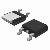
TRANS POWER PNP 8A 80V DPAK
Manufacturer
ON Semiconductor
Type
Powerr
Specifications of MJD45H11G
Transistor Type
PNP
Current - Collector (ic) (max)
8A
Voltage - Collector Emitter Breakdown (max)
80V
Vce Saturation (max) @ Ib, Ic
1V @ 400mA, 8A
Current - Collector Cutoff (max)
1µA
Dc Current Gain (hfe) (min) @ Ic, Vce
40 @ 4A, 1V
Power - Max
1.75W
Frequency - Transition
90MHz
Mounting Type
Surface Mount
Package / Case
DPak, TO-252 (2 leads+tab), SC-63
Transistor Polarity
PNP
Number Of Elements
1
Collector-emitter Voltage
80V
Emitter-base Voltage
5V
Collector Current (dc) (max)
8A
Dc Current Gain (min)
60
Power Dissipation
1.75W
Frequency (max)
90MHz
Operating Temp Range
-55C to 150C
Operating Temperature Classification
Military
Mounting
Surface Mount
Pin Count
2 +Tab
Package Type
DPAK
Configuration
Single
Mounting Style
SMD/SMT
Collector- Emitter Voltage Vceo Max
80 V
Emitter- Base Voltage Vebo
5 V
Continuous Collector Current
8 A
Maximum Dc Collector Current
8 A
Maximum Operating Frequency
90 MHz
Maximum Operating Temperature
+ 150 C
Dc Collector/base Gain Hfe Min
60 at 2 A at 1 V
Minimum Operating Temperature
- 55 C
Current, Collector
8 A
Current, Gain
40
Frequency
90 MHz
Polarity
PNP
Primary Type
Si
Resistance, Thermal, Junction To Case
6.25 °C/W
Voltage, Breakdown, Collector To Emitter
80 V
Voltage, Collector To Emitter
80 V
Voltage, Collector To Emitter, Saturation
1 V
Voltage, Emitter To Base
5 V
Lead Free Status / RoHS Status
Lead free / RoHS Compliant
Other names
MJD45H11G
MJD45H11GOS
MJD45H11GOS
Available stocks
Company
Part Number
Manufacturer
Quantity
Price
Company:

Part Number:
MJD45H11G
Manufacturer:
ON
Quantity:
2 300
Company:
Part Number:
MJD45H11G
Manufacturer:
ON
Quantity:
12 500
Company:
Part Number:
MJD45H11G
Manufacturer:
ON
Quantity:
12 500
Part Number:
MJD45H11G
Manufacturer:
ON/安森美
Quantity:
20 000


0.05
0.02
0.5
0.3
0.1
20
10
5
3
2
1
0.07
0.05
0.03
0.02
0.01
0.7
0.5
0.3
0.2
0.1
1
1
0.01
SINGLE PULSE
0.02
0.05
D = 0.5
V
0.02 0.03 0.05
Figure 2. Maximum Forward Bias
CE
0.2
0.1
, COLLECTOR-EMITTER VOLTAGE (VOLTS)
THERMAL LIMIT @ T
WIRE BOND LIMIT
3
Safe Operating Area
0.01
5
dc
7
0.1
5 ms
10
2.5
1.5
0.5
T
C
A
2
1
0
= 25°C
500 ms
T
25
20
15
10
0.2 0.3
5
0
C
25
20
30
100 ms
0.5
50
50
1 ms
Figure 1. Thermal Response
T
Figure 3. Power Derating
C
http://onsemi.com
SURFACE
70
MOUNT
1
T
T, TEMPERATURE (°C)
100
A
75
2
t, TIME (ms)
3
R
R
D CURVES APPLY FOR POWER
PULSE TRAIN SHOWN
READ TIME AT t
T
J(pk)
qJC(t)
qJC
3
a transistor: average junction temperature and second
breakdown. Safe operating area curves indicate I
limits of the transistor that must be observed for reliable
operation; i.e., the transistor must not be subjected to greater
dissipation than the curves indicate.
variable depending on conditions. Second breakdown pulse
limits are valid for duty cycles to 10% provided T
v 150_C. T
Figure 1. At high case temperatures, thermal limitations will
reduce the power that can be handled to values less than the
limitations imposed by second breakdown.
= 6.25°C/W MAX
- T
There are two limitations on the power handling ability of
The data of Figure 2 is based on T
= r(t) R
100
C
5
= P
qJC
(pk)
1
q
10
JC(t)
125
J(pk)
20
may be calculated from the data in
30
150
P
50
(pk)
DUTY CYCLE, D = t
t
1
100
t
2
J(pk)
200 300
= 150_C; T
1
/t
2
500
C
− V
J(pk)
C
1 k
CE
is
Related parts for MJD45H11G
Image
Part Number
Description
Manufacturer
Datasheet
Request
R

Part Number:
Description:
ON Semiconductor [VOLTAGE REGULATOR]
Manufacturer:
ON Semiconductor
Datasheet:
Part Number:
Description:
357-036-542-201 CARDEDGE 36POS DL .156 BLK LOPRO
Manufacturer:
ON Semiconductor
Datasheet:
Part Number:
Description:
357-036-542-201 CARDEDGE 36POS DL .156 BLK LOPRO
Manufacturer:
ON Semiconductor
Datasheet:
Part Number:
Description:
357-036-542-201 CARDEDGE 36POS DL .156 BLK LOPRO
Manufacturer:
ON Semiconductor
Datasheet:
Part Number:
Description:
357-036-542-201 CARDEDGE 36POS DL .156 BLK LOPRO
Manufacturer:
ON Semiconductor
Datasheet:
Part Number:
Description:
357-036-542-201 CARDEDGE 36POS DL .156 BLK LOPRO
Manufacturer:
ON Semiconductor
Datasheet:
Part Number:
Description:
357-036-542-201 CARDEDGE 36POS DL .156 BLK LOPRO
Manufacturer:
ON Semiconductor
Datasheet:
Part Number:
Description:
357-036-542-201 CARDEDGE 36POS DL .156 BLK LOPRO
Manufacturer:
ON Semiconductor
Datasheet:
Part Number:
Description:
357-036-542-201 CARDEDGE 36POS DL .156 BLK LOPRO
Manufacturer:
ON Semiconductor
Datasheet:
Part Number:
Description:
357-036-542-201 CARDEDGE 36POS DL .156 BLK LOPRO
Manufacturer:
ON Semiconductor
Datasheet:
Part Number:
Description:
357-036-542-201 CARDEDGE 36POS DL .156 BLK LOPRO
Manufacturer:
ON Semiconductor
Datasheet:
Part Number:
Description:
Manufacturer:
ON Semiconductor
Datasheet:
Part Number:
Description:
Manufacturer:
ON Semiconductor
Datasheet:
Part Number:
Description:
Manufacturer:
ON Semiconductor
Datasheet: