NUS5531MTR2G ON Semiconductor, NUS5531MTR2G Datasheet
NUS5531MTR2G
Specifications of NUS5531MTR2G
Available stocks


Related parts for NUS5531MTR2G

NUS5531MTR2G Summary of contents
Page 1
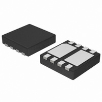
... Source Drain 5 4 (Bottom View) ORDERING INFORMATION Device Package Shipping NUS5531MTR2G WDFN8 3000/Tape & Reel (Pb−Free) †For information on tape and reel specifications, including part orientation and tape sizes, please refer to our Tape and Reel Packaging Specification Brochure, BRD8011/D. Publication Order Number: ...
Page 2
P−Channel Power MOSFET Maximum Ratings Drain−to−Source Voltage Gate−to−Source Voltage Continuous Drain Current (Note 1) Power Dissipation (Note 1) Continuous Drain Current (Note 2) Power Dissipation (Note 3) Pulsed Drain Current Operating Junction and Storage Temperature Operating Case Temperature (Note 3) ...
Page 3
P−Channel MOSFET Electrical Characteristics Parameter CHARGES, CAPACITANCES AND GATE RESISTANCE Input Capacitance Output Capacitance Reverse Transfer Capacitance Total Gate Charge Threshold Gate Charge Gate−to−Source Charge Gate−to−Drain Charge SWITCHING CHARACTERISTICS Turn−On Delay Time Rise Time Turn−Off Delay Time Fall Time DRAIN−SOURCE ...
Page 4
Single−PNP Transistor Electrical Characteristics Parameter OFF CHARACTERISTICS Collector−Emitter Breakdown Voltage Collector−Base Breakdown Voltage Emitter−Base Breakdown Voltage Collector−Emitter Cutoff Current ON CHARACTERISTICS DC Current Gain (Note 7) DC Current Gain (Note 7) Collector−Emitter Saturation Voltage Collector−Emitter Saturation Voltage Collector−Emitter Saturation Voltage ...
Page 5
TYPICAL CHARACTERISTICS − MOSFET −1.7 − −8 −V , DRAIN−TO−SOURCE VOLTAGE (V) DS Figure 3. On−Region Characteristics 0. 4 100°C J 0.04 ...
Page 6
TYPICAL CHARACTERISTICS − MOSFET 2800 2400 C iss 2000 1600 1200 C rss 800 C oss 400 0 −4 − −V − GATE−TO−SOURCE OR DRAIN−TO−SOURCE ...
Page 7
TYPICAL CHARACTERISTICS − MOSFET 0.5 0.2 0.1 0.1 0.05 0.02 0.01 0.01 Single Pulse 0.001 1E−06 1E−05 1E−04 1E−03 1E−02 1E−01 t, TIME (s) Figure 14. FET Thermal Response http://onsemi.com 7 1E+00 1E+01 1E+02 1E+03 ...
Page 8
TYPICAL CHARACTERISTICS − BJT 0.25 IC/ 0.2 0.15 0.1 0.05 0 0.001 0.01 0 COLLECTOR CURRENT (A) C Figure 15. Collector Emitter Saturation Voltage vs. Collector Current 600 150°C (5.0 V) 550 150°C (2.0 V) 500 ...
Page 9
TYPICAL CHARACTERISTICS − BJT 350 325 300 275 250 225 200 175 150 125 0 1.0 2.0 3.0 4 EMITTER BASE VOLTAGE (V) EB Figure 21. Input Capacitance 170 C (pF) ibo 150 130 110 ...
Page 10
... B NOTE 3 0.05 C *For additional information on our Pb−Free strategy and soldering details, please download the ON Semiconductor Soldering and Mounting Techniques Reference Manual, SOLDERRM/D. N. American Technical Support: 800−282−9855 Toll Free USA/Canada Europe, Middle East and Africa Technical Support: Phone: 421 33 790 2910 Japan Customer Focus Center Phone: 81− ...