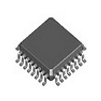
ICS8521BYI IDT, Integrated Device Technology Inc, ICS8521BYI Datasheet - Page 7

ICS8521BYI
Manufacturer Part Number
ICS8521BYI
Description
Manufacturer
IDT, Integrated Device Technology Inc
Type
Clock Driverr
Datasheet
1.ICS8521BYI.pdf
(15 pages)
Specifications of ICS8521BYI
Number Of Clock Inputs
2
Mode Of Operation
Differential
Output Frequency
500MHz
Output Logic Level
HSTL
Operating Supply Voltage (min)
3.135V
Operating Supply Voltage (typ)
3.3V
Operating Supply Voltage (max)
3.465V
Package Type
LQFP
Operating Temp Range
-40C to 85C
Operating Temperature Classification
Industrial
Mounting
Surface Mount
Pin Count
32
Lead Free Status / RoHS Status
Not Compliant
Available stocks
Company
Part Number
Manufacturer
Quantity
Price
Company:
Part Number:
ICS8521BYILF
Manufacturer:
IDT, Integrated Device Technology Inc
Quantity:
10 000
Company:
Part Number:
ICS8521BYILFT
Manufacturer:
IDT, Integrated Device Technology Inc
Quantity:
10 000
IDT™ / ICS™ LOW SKEW, 1-TO-9 DIFFERENTIAL-TO-HSTL FANOUT BUFFER
ICS8521I
LOW SKEW, 1-TO-9 DIFFERENTIAL-TO-HSTL FANOUT BUFFER
W
Figure 2 shows how the differential input can be wired to accept
single ended levels. The reference voltage V_REF = V
generated by the bias resistors R1, R2 and C1. This bias circuit
should be located as close as possible to the input pin. The ratio
R
I
CLK/nCLK I
For applications not requiring the use of the differential input,
both CLK and nCLK can be left floating. Though not required,
but for additional protection, a 1kΩ resistor can be tied from
CLK to ground.
PCLK/nPCLK I
For applications not requiring the use of a differential input,
both the PCLK and nPCLK pins can be left floating. Though
not required, but for additional protection, a 1kΩ resistor can
be tied from PCLK to ground.
LVCMOS C
All control pins have internal pull-ups or pull-downs; additional
resistance is not required but can be added for additional
protection. A 1kΩ resistor can be used.
8521BYI
NPUTS
ECOMMENDATIONS FOR
IRING THE
:
ONTROL
NPUT
NPUT
D
Integrated
Circuit
Systems, Inc.
:
IFFERENTIAL
P
:
INS
:
U
F
NUSED
IGURE
I
NPUT TO
2. S
I
NPUT AND
A
www.icst.com/products/hiperclocks.html
CLK_IN
INGLE
PPLICATION
A
0.1uF
CCEPT
C1
E
O
NDED
UTPUT
DD
S
/2 is
S
INGLE
IGNAL
P
R1
1K
V_REF
R2
1K
INS
7
7
I
NFORMATION
of R1 and R2 might need to be adjusted to position the V_REF in
the center of the input voltage swing. For example, if the input
clock swing is only 2.5V and V
and R2/R1 = 0.609.
O
HSTL O
All unused LVHSTL outputs can be left floating. We
recommend that there is no trace attached. Both sides of the
differential output pair should either be left floating or
terminated.
D
E
RIVING
UTPUTS
V
NDED
D
DD
+
-
IFFERENTIAL
UTPUT
D
:
L
IFFERENTIAL
EVELS
-
I
TO
NPUT
-HSTL F
DD
= 3.3V, V_REF should be 1.25V
L
OW
ANOUT
S
REV. A NOVEMBER 17, 2005
KEW
, 1-
B
UFFER
TO
ICS8521I
-9
TSD


