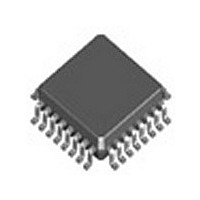
ICS85310AYI-11 IDT, Integrated Device Technology Inc, ICS85310AYI-11 Datasheet - Page 2

ICS85310AYI-11
Manufacturer Part Number
ICS85310AYI-11
Description
Manufacturer
IDT, Integrated Device Technology Inc
Type
Clock Driverr
Datasheet
1.ICS85310AYI-11.pdf
(18 pages)
Specifications of ICS85310AYI-11
Number Of Clock Inputs
2
Mode Of Operation
Differential
Output Frequency
700MHz
Output Logic Level
ECL/LVPECL
Operating Supply Voltage (min)
-2.375/2.375V
Operating Supply Voltage (typ)
-2.5/-3.3/3.3V
Operating Supply Voltage (max)
-3.8/3.8V
Package Type
LQFP
Operating Temp Range
-40C to 85C
Operating Temperature Classification
Industrial
Mounting
Surface Mount
Pin Count
32
Lead Free Status / RoHS Status
Not Compliant
Available stocks
Company
Part Number
Manufacturer
Quantity
Price
Company:
Part Number:
ICS85310AYI-11LF
Manufacturer:
IDT, Integrated Device Technology Inc
Quantity:
10 000
Company:
Part Number:
ICS85310AYI-11LFT
Manufacturer:
IDT, Integrated Device Technology Inc
Quantity:
10 000
Company:
Part Number:
ICS85310AYI-11T
Manufacturer:
IDT
Quantity:
9
Part Number:
ICS85310AYI-11T
Manufacturer:
IDT
Quantity:
20 000
ICS85310I-11 Data Sheet
Table 1. Pin Descriptions
NOTE: Pullup and Pulldown refer to internal input resistors. See Table 2, Pin Characteristics, for typical values.
Table 2. Pin Characteristics
ICS85310AYI-11 REVISION F JUNE 9, 2010
Symbol
C
R
R
9, 16, 25, 32
IN
PULLUP
PULLDOWN
Number
10, 11
12, 13
14, 15
17, 18
19, 20
21, 22
23, 24
26, 27
28, 29
30, 31
1
2
3
4
5
6
7
8
Parameter
Input Capacitance
Input Pullup Resistor
Input Pulldown Resistor
CLK_SEL
CLK_EN
nQ9, Q9
nQ8, Q8
nQ7, Q7
nQ6, Q6
nQ5, Q5
nQ4, Q4
nQ3, Q3
nQ2, Q2
nQ1, Q1
nQ0, Q0
nCLK0
nCLK1
Name
CLK0
CLK1
V
V
V
CCO
CC
EE
Output
Output
Output
Output
Output
Output
Output
Output
Output
Output
Power
Power
Power
Input
Input
Input
Input
Input
Input
Type
Pulldown
Pulldown
Pulldown
Pullup
Pullup
Pullup
Test Conditions
Description
Positive supply pin.
Clock select input. When HIGH, selects CLK1, nCLK1 inputs. When LOW,
selects CLK0, nCLK0 inputs. LVCMOS / LVTTL interface levels.
Non-inverting differential clock input.
Inverting differential clock input.
Synchronizing clock enable. When HIGH, clock outputs follow clock input.
When LOW, Q outputs are forced low, nQ outputs are forced high.
LVCMOS / LVTTL interface levels.
Non-inverting differential clock input.
Inverting differential clock input.
Negative supply pin.
Output supply pins.
Differential output pair. LVPECL interface levels.
Differential output pair. LVPECL interface levels.
Differential output pair. LVPECL interface levels.
Differential output pair. LVPECL interface levels.
Differential output pair. LVPECL interface levels.
Differential output pair. LVPECL interface levels.
Differential output pair. LVPECL interface levels.
Differential output pair. LVPECL interface levels.
Differential output pair. LVPECL interface levels.
Differential output pair. LVPECL interface levels.
LOW SKEW, 1-TO-10 DIFFERENTIAL-TO-3.3V, 2.5V LVPECL/ECL FANOUT BUFFER
2
Minimum
Typical
51
51
4
©2010 Integrated Device Technology, Inc.
Maximum
Units
k
k
pF
Ω
Ω


