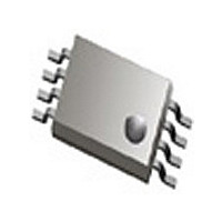
ICS853052AGT IDT, Integrated Device Technology Inc, ICS853052AGT Datasheet - Page 8

ICS853052AGT
Manufacturer Part Number
ICS853052AGT
Description
Manufacturer
IDT, Integrated Device Technology Inc
Type
Clock Multiplexerr
Datasheet
1.ICS853052AGT.pdf
(14 pages)
Specifications of ICS853052AGT
Number Of Clock Inputs
2
Mode Of Operation
Single-Ended
Output Logic Level
LVPECL
Operating Supply Voltage (min)
2.375V
Operating Supply Voltage (typ)
2.5/3.3/5V
Operating Supply Voltage (max)
5.5V
Package Type
TSSOP
Operating Temp Range
-40C to 85C
Operating Temperature Classification
Industrial
Signal Type
LVCMOS/LVTTL
Mounting
Surface Mount
Pin Count
8
Lead Free Status / RoHS Status
Not Compliant
T
The clock layout topology shown below is a typical termination
for LVPECL outputs. The two different layouts mentioned are
recommended only as guidelines.
FOUT and nFOUT are low impedance follower outputs that gen-
erate ECL/LVPECL compatible outputs. Therefore, terminating
resistors (DC current path to ground) or current sources must be
used for functionality. These outputs are designed to drive 50
IDT
T
This section shows examples of 5V LVPECL output termination.
Figure 3A shows standard termination for 5V LVPECL. The
termination requires matched load of 50
ERMINATION FOR
ICS853052
DUAL LVCMOS/LVTTL-TO-DIFFERENTIAL 2.5V, 3.3V, 5V LVPECL MULTIPLEXER
F
ERMINATION FOR
RTT =
™
IGURE
/ ICS
5V
™
((V
3A. S
F
2.5V, 3.3V, 5V LVPECL MULTIPLEXER
FOUT
OH
IGURE
PECL
+ V
OL
TANDARD
2A. LVPECL O
) / (V
Zo = 50 Ohm
Zo = 50 Ohm
1
3.3V LVPECL O
5V LVPECL O
CC
Z
Z
– 2)) – 2
o
o
5V LVPECL O
= 50
= 50
R1
50
Z
o
UTPUT
50
3V
UTPUT
T
UTPUTS
R2
50
UTPUT
ERMINATION
RTT
resistors pull down to
50
V
+
-
T
CC
ERMINATION
5V
FIN
- 2V
PECL
8
transmission lines. Matched impedance techniques should be
used to maximize operating frequency and minimize signal dis-
tortion. Figures 2A and 2B show two different layouts which are
recommended only as guidelines. Other suitable clock layouts
may exist and it would be recommended that the board design-
ers simulate to guarantee compatibility across all printed circuit
and clock component process variations.
V
equivalence of Figure 3A. In actual application where the 3V DC
power supply is not available, this approached is normally used.
CC
F
- 2V = 3V at the receiver. Figure 3B shows Thevenin
IGURE
FOUT
5V
F
3B. 5V LVPECL O
IGURE
PECL
2B. LVPECL O
Zo = 50 Ohm
Zo = 50 Ohm
Z
Z
o
o
= 50
= 50
ICS853052AG REV. B JANUARY 16, 2008
125
84
UTPUT
UTPUT
5V
R3
84
R1
125
3.3V
T
ERMINATION
R4
84
T
125
84
R2
125
ERMINATION
PRELIMINARY
FIN
+
-
E
XAMPLE
PECL


