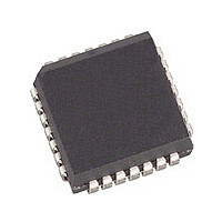
COM20020I-DZD Standard Microsystems (SMSC), COM20020I-DZD Datasheet - Page 9

COM20020I-DZD
Manufacturer Part Number
COM20020I-DZD
Description
Manufacturer
Standard Microsystems (SMSC)
Datasheet
1.COM20020I-DZD.pdf
(72 pages)
Specifications of COM20020I-DZD
Number Of Transceivers
1
Operating Supply Voltage (max)
5.5V
Operating Supply Voltage (typ)
5V
Operating Supply Voltage (min)
4.5V
Operating Temperature (max)
85C
Operating Temperature (min)
-40C
Operating Temperature Classification
Industrial
Mounting
Surface Mount
Pin Count
28
Lead Free Status / RoHS Status
Compliant
Available stocks
Company
Part Number
Manufacturer
Quantity
Price
Company:
Part Number:
COM20020I-DZD
Manufacturer:
Standard
Quantity:
17 665
Company:
Part Number:
COM20020I-DZD
Manufacturer:
SMSC
Quantity:
269
Company:
Part Number:
COM20020I-DZD
Manufacturer:
Microchip Technology
Quantity:
10 000
Company:
Part Number:
COM20020I-DZD-TR
Manufacturer:
Microchip Technology
Quantity:
10 000
5Mbps ARCNET (ANSI 878.1) Controller with 2K x 8 On-Chip RAM
Datasheet
Chapter 3
SMSC COM20020I Rev D
1-3
4-6,8-12
27
26
23
24
25
19,18
20
PLCC PIN
NO.
Data 0-7
Address
0-2
nRead/nData
Strobe
nWrite/
Direction
nReset in
nInterrupt
nChip Select
nPulse 2,
nPulse 1
Receive In
NAME
Description of Pin Functions
A0/nMUX,
A1,A2/ALE
AD0-AD2, D3-D7 Input/Output. On a non-multiplexed bus, these signals are
nRD/nDS
nWR/DIR
nRESET
nINTR
nCS
nPULSE2,
nPULSE1
RXIN
TRANSMISSION MEDIA INTERFACE
MICROCONTROLLER INTERFACE
SYMBOL
DATASHEET
Page 9
Input. On a non-multiplexed mode, A0-A2 are address
input bits. (A0 is the LSB) On a multiplexed address/data
bus, nMUX tied Low, A1 is left open, and ALE is tied to the
Address Latch Enable signal. A1 is connected to an internal
pull-up resistor.
used as the data lines for the device. On a multiplexed
address/data bus, AD0-AD2 act as the address lines
(latched by ALE) and as the low data lines for the device.
D3-D7 are always used for data only. These signals are
connected to internal pull-up resistors.
Input. On a 68XX-like bus, nDS is an active low signal
issued by the microcontroller as the data strobe signal to
strobe the data onto the bus. On a 80XX-like bus, nRD is
an active low signal issued by the microcontroller to
indicate a read operation.
Input. On a 68XX-like bus, DIR is issued by the
microcontroller as the Read/nWrite signal to determine the
direction of data transfer. In this case, a logic "1" selects a
read operation, while a logic "0" selects a write operation.
In this case, data is actually strobed by the nDS signal. On
an 80XX-like bus, nWR is an active low signal issued by
the microcontroller to indicate a write operation. In this
case, a logic "0" on this pin, when the COM20020ID is
accessed, enables data from the data bus to be written to
the device.
Output. This active low signal is generated by the
COM20020ID when an enabled interrupt condition occurs.
Input. This active low signal selects the COM20020ID for
an access.
Output (nPULSE1), Input/Output (nPULSE2). In Normal
Mode, these active low signals carry the transmit data
information, encoded in pulse format, as DIPULSE
waveform. When the device is in Backplane Mode, the
nPULSE1 signal driver is programmable (push/pull or open-
drain), while the nPULSE2 signal provides a clock with
frequency of double the data rate. nPULSE1 is connected
to a weak internal pull-up resistor on the open/drain driver
in backplane mode.
Input. This signal carries the receive data information from
the line transceiver.
Input. This active low signal executes a hardware reset.
DESCRIPTION
Revision 12-05-06


