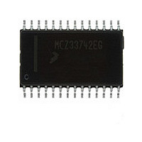
MCZ33742EG Freescale, MCZ33742EG Datasheet - Page 34

MCZ33742EG
Manufacturer Part Number
MCZ33742EG
Description
Manufacturer
Freescale
Datasheet
1.MCZ33742EG.pdf
(70 pages)
Specifications of MCZ33742EG
Data Rate
1000Kbps
Number Of Transceivers
1
Standard Supported
CAN 2.0
Operating Supply Voltage (max)
27V
Operating Supply Voltage (typ)
5/9/12/15/18/24V
Operating Supply Voltage (min)
4.5V
Package Type
SOIC W
Supply Current
45mA
Operating Temperature (max)
125C
Operating Temperature (min)
-40C
Operating Temperature Classification
Automotive
Mounting
Surface Mount
Pin Count
28
Lead Free Status / RoHS Status
Compliant
Available stocks
Company
Part Number
Manufacturer
Quantity
Price
Part Number:
MCZ33742EG
Manufacturer:
FREESCALE
Quantity:
20 000
Part Number:
MCZ33742EGR2
Manufacturer:
FREESCALE
Quantity:
20 000
DEBUG MODE: HARDWARE AND SOFTWARE
DEBUG WITH THE 33742
printed circuit board, both the MCU software and the 33742
operation must be debugged concurrently. The following
features permit system debugging by allowing the disabling
of the SBC internal software watchdog timer.
DEVICE POWER-UP, RESET PIN CONNECTED TO
VDD
but the 33742 will not have received any SPI communication
to configure itself. Until set up by the system MCU, the 33742
will generate a reset every 350ms until the part is configured.
To avoid continuous MCU hardware resets, the 33742’s RST
pin can be connected directly to the VDD pin by a hardware
jumper.
DEBUG MODES WITH SOFTWARE WATCHDOG
DISABLED THOUGH SPI (NORMAL DEBUG,
STANDBY DEBUG, AND STOP DEBUG)
through the SPI. To set the watchdog disable while limiting
the risk of inadvertently disabling the watchdog timer during
been set into Stop Debug or Sleep mode, a wake-up causes
the 33742 to enter the Normal Request mode for 350ms. To
avoid having the SBC generate an unwanted reset (enter
Reset mode), the next debug mode (Normal Debug or
Standby Debug) should be configured within the 350ms time
window of the Normal Request mode.
34
33742
FUNCTIONAL DEVICE OPERATION
OPERATIONAL MODES
When a SBC, and the MCU it serves, is used on the same
The VDD voltage is available when the 33742 power-up
The software configurable watchdog can be disabled
When the SBC is operating in the debug mode and has
Debug Mode
BATFAIL
V
V
SUP
DD
SPI
TIM1(Step 3)
MCR (Step 4)
MCR (Step 5)
Figure 15. Entering Debug Mode
SPI: Read BATFAIL
33742 in Debug mode.
No Watchdog
normal 33742 operation, it is recommended that the disable
be done using the following sequence:
• Step 1– Power down the SBC.
• Step 2 – Power up the SBC. This sets the BATFAIL bit,
• Step 3 – Write to the TIM1 sub register to allow the SBC to
• Step 4 – Write to the MCR register with data 0000. This
• Step 5 – Write to the MCR register normal debug. SPI byte
• Step 6 – To leave the debug mode, write 0000 to the MCR
should be completed consecutively and within the 350ms
time period of the Normal Request mode. If not, the 33742
will go into Reset mode and enter Normal Request again.
the BATFAIL bit (MCR read) and write 0000 into the MCR
register.
of the SBC once the debug mode has been selected.
allowing the 33742 to enter Normal Request mode.
enter Normal mode.
enables the debug mode. Complete SPI byte is
0001 0000.
is 0001 x101.
without having to clear the watchdog on a regular basis to
facilitate software and hardware debug.
register.
At Step 2, the SBC is in Normal Request. Steps 3, 4, and 5
Figure
To avoid entering debug mode after a power-up, first read
Figures 16 and 17, page 35, show the detailed operation
Important While in debug mode, the SBC can be used
15, page 34, illustrates debug mode selection.
MCR (Step 6)
Analog Integrated Circuit Device Data
33742 not in Debug mode.
Watchdog ON
Freescale Semiconductor


