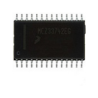
MCZ33742EG Freescale, MCZ33742EG Datasheet - Page 37

MCZ33742EG
Manufacturer Part Number
MCZ33742EG
Description
Manufacturer
Freescale
Datasheet
1.MCZ33742EG.pdf
(70 pages)
Specifications of MCZ33742EG
Data Rate
1000Kbps
Number Of Transceivers
1
Standard Supported
CAN 2.0
Operating Supply Voltage (max)
27V
Operating Supply Voltage (typ)
5/9/12/15/18/24V
Operating Supply Voltage (min)
4.5V
Package Type
SOIC W
Supply Current
45mA
Operating Temperature (max)
125C
Operating Temperature (min)
-40C
Operating Temperature Classification
Automotive
Mounting
Surface Mount
Pin Count
28
Lead Free Status / RoHS Status
Compliant
Available stocks
Company
Part Number
Manufacturer
Quantity
Price
Part Number:
MCZ33742EG
Manufacturer:
FREESCALE
Quantity:
20 000
Part Number:
MCZ33742EGR2
Manufacturer:
FREESCALE
Quantity:
20 000
CAN PHYSICAL INTERFACE
simplified block diagram of the CAN interface of the 33742.
CAN INTERFACE SUPPLY
The CAN interface also has a supply path from the external
supply line through the VSUP pin. This path is used in CAN
Sleep mode to allow wake-up detection.
the CAN interface current is sourced from the V2 pin. During
CAN low power mode, the current is sourced from the VSUP
pin.
MAIN OPERATION MODES DESCRIPTION
modes: TXRX and Sleep mode. The modes are controlled by
the CAN SPI Register. In the TXRX mode, which is used for
communication, four different slew rates are available for the
user. In the Sleep mode, the user has the option of enabling
or disabling the remote CAN wake-up capability.
Analog Integrated Circuit Device Data
Freescale Semiconductor
The SBC features a high-speed CAN physical interface for bus communication from 60kbps up to 1.0Mbps.
The supply voltage for the CAN transceiver is the V2 pin.
During CAN communication (transmission and reception),
The CAN interface of the SBC has two main operating
VSUP
RXD
TXD
Wake-up
Internal
Signal
V2
Figure 19. Simplified Block Diagram of CAN Interface
SPI Control
SPI Control
Differential
Receiver
V2
Recognition
Wake-up
Pattern
SPI Control
33742
2.5 V
Driver
Driver
V2
V2
Wake-up
Receiver
CAN DRIVER OPERATION IN TXRX MODE
two states: recessive or dominant. The driver state is
controlled by the TXD pin. The bus state is reported through
the RXD pin.
CANH and CANL lines are biased to the voltage set at V2
divided by 2, or approximately 2.5V.
CANL and CANH drivers are active. CANL is pulled to
ground, and CANH is pulled HIGH toward 5.0V (voltage at
V2).
voltage is compared versus an internal threshold (a few
hundred millivolts). If CANH minus CANL is below the
threshold, the bus is recessive and RXD is set HIGH. If CANH
minus CANL is above the threshold, the bus is dominant and
RXD is set LOW. This is illustrated in
V2
When the CAN interface is in TXRX mode, the driver has
When TXD is HIGH, the driver is set in recessive state, and
When TXD is LOW, the bus is set into dominant state:
The RXD pin reports the bus state: CANH minus CANL
QL
QH
CANH
CANL
FUNCTIONAL DEVICE OPERATION
Bus Termination (60Ω)
CANH Line
CANL Line
OPERATIONAL MODES
Figure
Figure 19
19.
is a
33742
37


