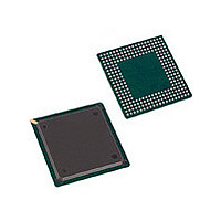
CYP15G0402DXB-BGI Cypress Semiconductor Corp, CYP15G0402DXB-BGI Datasheet - Page 13

CYP15G0402DXB-BGI
Manufacturer Part Number
CYP15G0402DXB-BGI
Description
Manufacturer
Cypress Semiconductor Corp
Datasheet
1.CYP15G0402DXB-BGI.pdf
(29 pages)
Specifications of CYP15G0402DXB-BGI
Lead Free Status / RoHS Status
Not Compliant
Document #: 38-02057 Rev. *G
When configured for local loopback (LPENx = HIGH), the
output drivers for all enabled ports are configured to drive a
static differential logic-1.
Each output can be enabled or disabled separately through
the BOE[7:0] inputs, as controlled by the OELE latch-enable
signal. When OELE is HIGH, the signals present on the
BOE[7:0] inputs are passed through the Serial Output Enable
Latch to control the Serial Output Drivers. The BOE[7:0] input
associated with a specific OUTx± driver is listed in Table 2.
When OELE is HIGH and BOE[x] is HIGH, the associated
Serial Driver is enabled. When OELE is HIGH and BOE[x] is
LOW, the associated driver is disabled and internally powered
down, the associated internal logic for that channel is also
powered down. When OELE returns LOW, the values present
on the BOE[7:0] inputs are latched in the Output Enable Latch,
and remain there until OELE returns HIGH to enable the latch.
A device reset (TRSTZ sampled LOW) clears this latch and
disables all output drivers.
Transmit PLL Clock Multiplier
The Transmit PLL Clock Multiplier accepts a character-rate or
half-character-rate external clock at the REFCLK input, and
multiples that clock by 10 or 20 (as selected by TXRATE) to
generate a bit-rate clock for use by the Transmit Shifter. It also
provides a character-rate clock used by the transmit paths.
The clock multiplier PLL can accept a REFCLK input between
19.5 MHz and 150 MHz, however, this clock range is limited
by the operating mode of the CYP(V)15G0402DXB clock
multiplier (controlled by TXRATE) and by the level on the
SPDSEL input.
When TXCKSEL = MID or HIGH (TXCLKx or TXCLKA
selected to clock input register), TXRATE = HIGH (Half-rate
REFCLK) is an invalid mode of operation.
SPDSEL is a three-level select
one of three operating ranges for the serial data outputs and
inputs. The operating serial signaling-rate and allowable range
of REFCLK frequencies is listed in Table 3.
Table 3. Operating Speed Settings
Note:
8.
MID (Open)
SPDSEL
NOTE: When all transmit channels are disabled (i.e., both
serial output drivers disabled in all channels) and a serial
output driver is re-enabled, the data on the Serial Drivers
may not meet all timing specifications for up to 200 µs.
REFCLK has no phase or frequency relationship with the recovered clock(s) and only acts as a centering reference to reduce clock synchronization time. REFCLK
must be within ±1500 PPM (±0.15%) of the remote transmitter’s PLL reference (REFCLK) frequency. Although transmitting to a HOTLink II receiver necessitates
the frequency difference between the transmitter and receiver reference clocks to be within ±1500 ppm, the stability of the crystal needs to be within the limits
specified by the appropriate standard when transmitting to a remote receiver that is compliant to that standard. For example, to be IEEE 802.3z Gigabit Ethernet
compliant, the frequency stability of the crystal needs to be within ±100 ppm.
HIGH
LOW
TXRATE
1
0
1
0
1
0
Frequency
[5]
REFCLK
reserved
19.5–40
80–150
20–40
40–75
(MHz)
40–80
(ternary) input that selects
Rate (MBaud)
Signaling
800–1500
400–800
195-400
The REFCLK± input is a differential input with each input inter-
nally biased to 1.4V. If the REFCLK+ input is connected to a
TTL, LVTTL, or LVCMOS clock source, the input signal is
recognized when it passes through the internally biased
reference point and REFCLK- can be left floating.
When both the REFCLK+ and REFCLK– inputs are
connected, the clock source must be a differential clock. This
can be either a differential LVPECL clock that is DC- or
AC-coupled, or a differential LVTTL or LVCMOS clock.
By connecting the REFCLK– input to an external voltage
source or resistive voltage divider, it is possible to adjust the
reference point of the REFCLK+ input for alternate logic levels.
When doing so it is necessary to ensure that the input differ-
ential crossing point remains within the parametric range
supported by the input.
CYP(V)15G0402DXB Receive Data Path
Serial Line Receivers
A differential line receiver, INx±, is available on each channel
for accepting a serial bit stream. The Serial Line Receiver
inputs are differential, and can accommodate wire inter-
connect and filtering losses or transmission line attenuation
greater than 16 dB. For normal operation, these inputs should
receive a signal of at least VI
peak-to-peak differential. Each Line Receiver can be DC- or
AC-coupled to +3.3V powered fiber-optic interface modules
(any ECL/PECL family, not limited to 100K PECL) or
AC-coupled
common-mode tolerance of these line receivers accommo-
dates a wide range of signal termination voltages. Each
receiver provides internal DC-restoration, to the center of the
receiver’s common mode range, for AC-coupled signals.
The local loopback inputs (LPENx) for each channel allows the
serial transmit data outputs to be routed internally back to the
Clock and Data Recovery circuit associated with that channel.
When configured for local loopback, all transmit Serial Driver
outputs are forced to output a differential logic-1. This prevents
local diagnostic patterns from being broadcast to attached
remote receivers.
Signal Detect/ Link Fault
Each selected Line Receiver is simultaneously monitored for
All of these conditions must be valid for the Signal Detect block
to indicate a valid signal is present. This status is presented on
the LFIx (Link Fault Indicator) output associated with each
receive channel.
• analog amplitude above limit specified by SDASEL
• transition density greater than specified limit
• CDR tracking data within expected frequency range as
• receive channel enabled
defined by REFCLK and TXRATE (± 1500 ppm)
to
+5V
powered
CYP15G0402DXB
CYV15G0402DXB
DIFF
optical
> 100 mV, or 200 mV
modules.
Page 13 of 29
[8]
The
[+] Feedback


