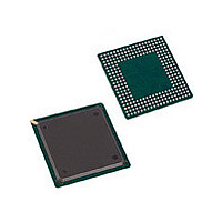
CYP15G0402DXB-BGI Cypress Semiconductor Corp, CYP15G0402DXB-BGI Datasheet - Page 8

CYP15G0402DXB-BGI
Manufacturer Part Number
CYP15G0402DXB-BGI
Description
Manufacturer
Cypress Semiconductor Corp
Datasheet
1.CYP15G0402DXB-BGI.pdf
(29 pages)
Specifications of CYP15G0402DXB-BGI
Lead Free Status / RoHS Status
Not Compliant
Document #: 38-02057 Rev. *G
Pin Descriptions
TXRATE
TXRST
Receive Path Data Signals
RXDA[9:0]
RXDB[9:0]
RXDC[9:0]
RXDD[9:0]
COMDETA
COMDETB
COMDETC
COMDETD
RXOPA
RXOPB
RXOPC
RXOPD
RFENA
RFENB
RFENC
RFEND
RXRATE
Receive Path Clock and Clock Control
Name
LVTTL Input,
asynchronous,
internal pull-up
LVTTL Input,
asynchronous,
internal pull-up,
sampled by
REFCLK↑
LVTTL Output,
synchronous to the
selected RXCLKx↑
LVTTL Output,
synchronous to the
selected RXCLKx↑
Three-state, LVTTL
Output, synchronous
to the selected
RXCLKx↑ output
LVTTL Input,
asynchronous,
internal pull-down
LVTTL Input
Static Control Input
I/O Characteristics Signal Description
CYP(V)15G0402DXB Quad HOTLink II™ SERDES (continued)
[4]
Transmit PLL Clock Rate Select. When TXRATE = HIGH, the Transmit PLL multiplies
REFCLK by 20 to generate the serial bit-rate clock. When TXRATE = LOW, the transmit
PLL multiples REFCLK by 10 to generate the serial bit-rate clock. See Table 3 for a list
of operating serial rates.
When TXCKSEL = MID or HIGH (TXCLKx or TXCLKA selected to clock input register),
TXRATE = HIGH (Half-rate REFCLK) is an invalid mode of operation.
Transmit Clock Phase Reset. Active LOW. When sampled LOW, the transmit
Phase-align Buffers are allowed to adjust their data-transfer timing (relative to the
selected input clock) to allow clean transfer of data from the Input Register to the
Transmit Shifter. When TXRST is sampled HIGH, the internal phase relationship
between the associated TXCLKx and the internal character-rate clock is fixed and the
device operates normally.
When configured for half-rate REFCLK sampling of the transmit character stream
(TXCKSEL = LOW and TXRATE = HIGH), assertion of TXRST is only used to clear
Phase-align buffer faults caused by highly asymmetric REFCLK periods or REFCLKs
with excessive cycle-to-cycle jitter. During this alignment period, one or more characters
may be added to or lost from all the associated transmit paths as the transmit
Phase-align Buffers are adjusted. TXRST must be sampled LOW by a minimum of two
consecutive rising edges of REFCLK to ensure the reset operation is initiated correctly
on all channels. This input is ignored when both TXCKSEL and TXRATE are LOW, since
the phase align buffer is bypassed. In all other configurations, TXRST should be
asserted during device initialization to ensure proper operation of the Phase-align buffer.
TXRST should be asserted after the assertion and deassertion of TRSTZ, after the
presence of a valid TXCLKx and after allowing enough time for the TXPLL to lock to the
reference clock (as specified by parameter t
Receive Data Output. These outputs change following the rising edge of the selected
receive interface clock.
Frame Character Detected. COMDETx = HIGH indicates the presence of a Framing
character in that Output Register.
Receive Path Odd Parity. When parity generation is enabled (PARCTL ≠ LOW), the
parity output at these pins is valid for the data on the associated RXDx bus bits. When
parity generation is disabled (PARCTL = LOW) these output drivers are disabled
(High-Z).
Reframe Enable. Active HIGH. When HIGH the framer for the associated channel is
enabled to frame as per the presently enabled framing mode and selected framing
character.
Receive Clock Rate Select.When LOW, the RXCLKx± recovered clock outputs are
complementary clocks operating at the recovered character rate. Data for the associated
receive channels should be latched on the rising edge of RXCLKx+ or falling edge of
RXCLKx–.
When HIGH, the RXCLKx± recovered clock outputs are complementary clocks
operating at half the character rate. Data for the associated receive channels should be
latched alternately on the rising edge of RXCLKx+ and RXCLKx–.
TXLOCK
).
CYP15G0402DXB
CYV15G0402DXB
Page 8 of 29
[+] Feedback


