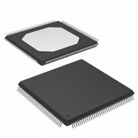
XC95144XL-10TQG144I Xilinx Inc, XC95144XL-10TQG144I Datasheet - Page 5

XC95144XL-10TQG144I
Manufacturer Part Number
XC95144XL-10TQG144I
Description
CPLD XC9500XL Family 3.2K Gates 144 Macro Cells 100MHz 0.35um (CMOS) Technology 3.3V 144-Pin TQFP
Manufacturer
Xilinx Inc
Series
XC9500XLr
Specifications of XC95144XL-10TQG144I
Package
144TQFP
Family Name
XC9500XL
Device System Gates
3200
Maximum Propagation Delay Time
10 ns
Number Of User I/os
117
Number Of Logic Blocks/elements
8
Typical Operating Supply Voltage
3.3 V
Maximum Operating Frequency
100 MHz
Number Of Product Terms Per Macro
90
Memory Type
Flash
Operating Temperature
-40 to 85 °C
Programmable Type
In System Programmable (min 10K program/erase cycles)
Delay Time Tpd(1) Max
10.0ns
Voltage Supply - Internal
3 V ~ 3.6 V
Number Of Logic Elements/blocks
8
Number Of Macrocells
144
Number Of Gates
3200
Number Of I /o
117
Mounting Type
Surface Mount
Package / Case
144-TQFP, 144-VQFP
Voltage
3.3V
Lead Free Status / RoHS Status
Lead free / RoHS Compliant
Features
-
Number Of Logic Elements/cells
-
Lead Free Status / RoHS Status
Lead free / RoHS Compliant
Other names
122-1375
Available stocks
Company
Part Number
Manufacturer
Quantity
Price
Company:
Part Number:
XC95144XL-10TQG144I
Manufacturer:
Xilinx Inc
Quantity:
10 000
AC Characteristics
DS056 (v2.0) April 3, 2007
Product Specification
Device Output
Symbol
f
T
Symbol
SYSTEM
T
APRPW
T
T
T
T
T
T
T
T
T
T
T
T
T
C
T
WLH
I
PSU
PCO
POE
POD
PAO
PLH
I
CO
OE
OD
AO
CC
PD
SU
PH
IH
H
IN
R
I/O to output valid
I/O setup time before GCK
I/O hold time after GCK
GCK to output valid
Multiple FB internal operating frequency
I/O setup time before p-term clock input
I/O hold time after p-term clock input
P-term clock output valid
GTS to output valid
GTS to output disable
Product term OE to output enabled
Product term OE to output disabled
GSR to output valid
P-term S/R to output valid
GCK pulse width (High or Low)
Asynchronous preset/reset pulse width
(High or Low)
P-term clock pulse width (High or Low)
I/O high-Z leakage current
I/O capacitance
Operating supply current
(low power mode, active)
V
TEST
R
R
1
2
Parameter
Parameter
C
L
Figure 3: AC Load Circuit
Output Type
www.xilinx.com
V
V
V
V
V
CC
IN
CC
IN
IN
= GND or 3.6V
= GND; f = 1.0 MHz
= GND, No load; f = 1.0 MHz
= Max; V
Min < V
XC95144XL-5
Min
3.7
1.7
2.0
2.8
5.0
5.0
0
-
-
-
-
-
-
-
-
-
-
Test Conditions
IN
CCIO
V
3.3V
2.5V
178.6
< 5.5V
CCIO
Max
10.0
10.5
5.0
3.5
5.5
4.0
4.0
7.0
7.0
-
-
-
-
-
-
-
= Max;
XC95144XL-7
Min
V
4.8
1.6
3.2
4.0
6.5
6.5
3.3V
2.5V
0
TEST
-
-
-
-
-
-
-
-
-
-
XC95144XL High Performance CPLD
125.0
Max
12.0
12.6
7.5
4.5
7.7
5.0
5.0
9.5
9.5
-
-
-
-
-
-
-
320 Ω
250 Ω
R
1
Min
45 (Typical)
-
-
-
XC95144XL-10
Min
6.5
2.1
4.4
4.5
7.0
7.0
0
-
-
-
-
-
-
-
-
-
-
360 Ω
660 Ω
R
2
100.0
Max
±10
±50
Max
10.0
10.2
14.5
15.3
11.0
11.0
10
5.8
7.0
7.0
-
-
-
-
-
-
-
DS058_03_081500
35 pF
35 pF
Units
C
Units
MHz
mA
μA
μA
pF
L
ns
ns
ns
ns
ns
ns
ns
ns
ns
ns
ns
ns
ns
ns
ns
ns
5


