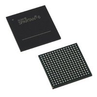
XC6SLX16-2FTG256C Xilinx Inc, XC6SLX16-2FTG256C Datasheet - Page 68

XC6SLX16-2FTG256C
Manufacturer Part Number
XC6SLX16-2FTG256C
Description
FPGA, SPARTAN-6 LX, 14K, 256FTGBGA
Manufacturer
Xilinx Inc
Series
Spartan® 6 LXr
Specifications of XC6SLX16-2FTG256C
No. Of Logic Blocks
2278
No. Of Macrocells
14579
Family Type
Spartan-6
No. Of Speed Grades
2
Total Ram Bits
589824
No. Of I/o's
186
Clock Management
DCM, PLL
I/o Supply Voltage
3.3V
Number Of Logic Elements/cells
14579
Number Of Labs/clbs
1139
Number Of I /o
186
Voltage - Supply
1.14 V ~ 1.26 V
Mounting Type
Surface Mount
Operating Temperature
0°C ~ 85°C
Package / Case
256-LBGA
Package
256FTBGA
Family Name
Spartan®-6
Device Logic Cells
14579
Device Logic Units
9112
Number Of Registers
18224
Typical Operating Supply Voltage
1.2 V
Maximum Number Of User I/os
186
Ram Bits
589824
Core Supply Voltage Range
1.14V
Rohs Compliant
Yes
Lead Free Status / RoHS Status
Lead free / RoHS Compliant
Number Of Gates
-
Lead Free Status / RoHS Status
Lead free / RoHS Compliant, Lead free / RoHS Compliant
Other names
122-1672
Available stocks
Company
Part Number
Manufacturer
Quantity
Price
Company:
Part Number:
XC6SLX16-2FTG256C
Manufacturer:
TI
Quantity:
21 500
Company:
Part Number:
XC6SLX16-2FTG256C
Manufacturer:
Xilinx Inc
Quantity:
10 000
Table 74: Global Clock Setup and Hold With DCM and PLL in Source-Synchronous Mode
DS162 (v2.0) March 31, 2011
Preliminary Product Specification
Notes:
1.
2.
Example Data Input Set-Up and Hold Times Relative to a Forwarded Clock Input Pin,
situations where clock and data inputs conform to different standards, adjust the setup and hold values accordingly using the values
shown in
T
T
PSDCMPLL_0
PHDCMPLL_0
Setup and Hold times are measured over worst case conditions (process, voltage, temperature). Setup time is measured relative to the Global Clock
input signal using the slowest process, highest temperature, and lowest voltage. Hold time is measured relative to the Global Clock input signal using
the fastest process, lowest temperature, and highest voltage. The timing values were measured using the fine-phase adjustment feature of the DCM.
These measurements include CMT jitter; DCM CLK0 driving PLL, PLL CLKOUT0 driving BUFG. Package skew is not included in these
measurements.
IFF = Input Flip-Flop
Symbol
IOB Switching Characteristics, page
/
No Delay Global Clock and IFF
Source-Synchronous Mode and PLL in
DCM2PLL Mode.
Description
20.
(2)
with DCM in
www.xilinx.com
Spartan-6 FPGA Data Sheet: DC and Switching Characteristics
XC6SLX4
XC6SLX9
XC6SLX16
XC6SLX25
XC6SLX25T
XC6SLX45
XC6SLX45T
XC6SLX75
XC6SLX75T
XC6SLX100
XC6SLX100T
XC6SLX150
XC6SLX150T
Device
(1)
Using DCM, PLL, and Global Clock Buffer. For
0.43/
0.43/
0.74/
0.67/
0.84/
0.65/
0.67/
0.86/
0.89/
0.50/
0.63/
0.45/
0.50/
1.07
1.03
0.93
1.02
1.02
0.99
1.00
1.01
1.03
1.10
1.10
1.28
1.28
-3
0.45/
0.74/
0.76/
0.84/
0.65/
0.67/
0.88/
0.89/
0.56/
0.63/
0.47/
0.50/
1.14
1.12
1.11
1.11
1.04
1.04
1.06
1.06
1.10
1.10
1.28
1.28
Speed Grade
- 3N
N/A
0.43/
0.45/
0.74/
0.84/
0.84/
0.71/
0.71/
0.94/
0.94/
0.61/
0.63/
0.52/
0.52/
1.43
1.43
1.21
1.18
1.18
1.12
1.12
1.14
1.14
1.17
1.17
1.28
1.28
- 2
1.10/
1.10/
0.77/
1.23/
1.18/
0.84/
1.27/
1.67
1.67
1.35
1.46
1.58
1.29
1.67
2.24
1.56
N/A
N/A
N/A
N/A
N/A
-1L
Units
ns
ns
ns
ns
ns
ns
ns
ns
ns
ns
ns
ns
ns
68


