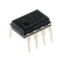
PIC12LF1840-E/P Microchip Technology, PIC12LF1840-E/P Datasheet - Page 268

PIC12LF1840-E/P
Manufacturer Part Number
PIC12LF1840-E/P
Description
7 KB Flash, 256 Bytes RAM, 32 MHz Int. Osc, 6 I/0, Enhanced Mid Range Core, Nano
Manufacturer
Microchip Technology
Series
PIC® XLP™ 12Fr
Datasheet
1.PIC12F1840-EMF.pdf
(382 pages)
Specifications of PIC12LF1840-E/P
Processor Series
PIC12F
Core
PIC
Program Memory Type
Flash
Program Memory Size
7 KB
Data Ram Size
256 B
Interface Type
MI2C, SPI, EUSART
Number Of Timers
3
Operating Supply Voltage
1.8 V to 5.5 V
Maximum Operating Temperature
+ 125 C
Mounting Style
Through Hole
Package / Case
PDIP-8
Development Tools By Supplier
MPLAB IDE Software
Minimum Operating Temperature
- 40 C
Core Processor
RISC
Core Size
8-Bit
Speed
32MHz
Connectivity
I²C, LIN, SPI, UART/USART
Peripherals
Brown-out Detect/Reset, POR, PWM, WDT
Number Of I /o
5
Eeprom Size
256 x 8
Ram Size
256 x 8
Voltage - Supply (vcc/vdd)
1.8 V ~ 3.6 V
Data Converters
A/D 4x10b
Oscillator Type
Internal
Operating Temperature
-40°C ~ 125°C
Lead Free Status / Rohs Status
Details
- Current page: 268 of 382
- Download datasheet (4Mb)
PIC12(L)F1840
FIGURE 26-2:
The operation of the EUSART module is controlled
through three registers:
• Transmit Status and Control (TXSTA)
• Receive Status and Control (RCSTA)
• Baud Rate Control (BAUDCON)
These
Register 26-2
When the receiver or transmitter section is not enabled
then the corresponding RX or TX pin may be used for
general purpose input and output.
DS41441B-page 268
BRG16
Baud Rate Generator
SPBRGH
registers
and
SPBRGL
Register
RX/DT pin
are
+ 1
EUSART RECEIVE BLOCK DIAGRAM
detailed
26-3, respectively.
Multiplier
BRG16
SYNC
BRGH
Pin Buffer
and Control
in
SPEN
1 X 0 0
X 1 1 0
X 1 0 1
x4
Register
x16 x64
F
OSC
0
0
0
26-1,
Preliminary
n
Data
Recovery
÷ n
FERR
Stop
MSb
CREN
(8)
RX9D
7
RX9
RSR Register
2011 Microchip Technology Inc.
RCREG Register
• • •
OERR
8
1
RCIF
RCIE
Data Bus
0
START
LSb
RCIDL
Interrupt
FIFO
Related parts for PIC12LF1840-E/P
Image
Part Number
Description
Manufacturer
Datasheet
Request
R

Part Number:
Description:
Manufacturer:
Microchip Technology Inc.
Datasheet:

Part Number:
Description:
Manufacturer:
Microchip Technology Inc.
Datasheet:

Part Number:
Description:
Manufacturer:
Microchip Technology Inc.
Datasheet:

Part Number:
Description:
Manufacturer:
Microchip Technology Inc.
Datasheet:

Part Number:
Description:
Manufacturer:
Microchip Technology Inc.
Datasheet:

Part Number:
Description:
Manufacturer:
Microchip Technology Inc.
Datasheet:

Part Number:
Description:
Manufacturer:
Microchip Technology Inc.
Datasheet:

Part Number:
Description:
Manufacturer:
Microchip Technology Inc.
Datasheet:


