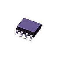
PIC12LF1840-E/SN Microchip Technology, PIC12LF1840-E/SN Datasheet - Page 352

PIC12LF1840-E/SN
Manufacturer Part Number
PIC12LF1840-E/SN
Description
7 KB Flash, 256 Bytes RAM, 32 MHz Int. Osc, 6 I/0, Enhanced Mid Range Core, Nano
Manufacturer
Microchip Technology
Series
PIC® XLP™ 12Fr
Datasheet
1.PIC12F1840-EMF.pdf
(382 pages)
Specifications of PIC12LF1840-E/SN
Processor Series
PIC12F
Core
PIC
Program Memory Type
Flash
Program Memory Size
7 KB
Data Ram Size
256 B
Interface Type
MI2C, SPI, EUSART
Number Of Timers
3
Operating Supply Voltage
1.8 V to 5.5 V
Maximum Operating Temperature
+ 125 C
Mounting Style
SMD/SMT
Package / Case
SOIC-8
Development Tools By Supplier
MPLAB IDE Software
Minimum Operating Temperature
- 40 C
Core Processor
RISC
Core Size
8-Bit
Speed
32MHz
Connectivity
I²C, LIN, SPI, UART/USART
Peripherals
Brown-out Detect/Reset, POR, PWM, WDT
Number Of I /o
5
Eeprom Size
256 x 8
Ram Size
256 x 8
Voltage - Supply (vcc/vdd)
1.8 V ~ 3.6 V
Data Converters
A/D 4x10b
Oscillator Type
Internal
Operating Temperature
-40°C ~ 125°C
Lead Free Status / Rohs Status
Details
Available stocks
Company
Part Number
Manufacturer
Quantity
Price
Company:
Part Number:
PIC12LF1840-E/SN
Manufacturer:
MICRON
Quantity:
4 500
- Current page: 352 of 382
- Download datasheet (4Mb)
PIC12(L)F1840
TABLE 30-15: I
DS41441B-page 352
Note 1:
Param.
SP100* T
SP101* T
SP102* T
SP103* T
SP106* T
SP107* T
SP109* T
SP110* T
SP111
No.
2:
*
These parameters are characterized but not tested.
As a transmitter, the device must provide this internal minimum delay time to bridge the undefined region
(min. 300 ns) of the falling edge of SCLx to avoid unintended generation of Start or Stop conditions.
A Fast mode (400 kHz) I
the requirement T
not stretch the low period of the SCLx signal. If such a device does stretch the low period of the SCLx sig-
nal, it must output the next data bit to the SDAx line T
to the Standard mode I
C
Symbol
SU
AA
R
HIGH
LOW
F
HD
BUF
B
:
:
DAT
DAT
2
C™ BUS DATA REQUIREMENTS
Clock high time
Clock low time
SDAx and SCLx
rise time
SDAx and SCLx fall
time
Data input hold time 100 kHz mode
Data input setup
time
Output valid from
clock
Bus free time
Bus capacitive loading
SU
:
DAT
Characteristic
2
C bus specification), before the SCLx line is released.
2
250 ns must then be met. This will automatically be the case if the device does
C
™
bus device can be used in a Standard mode (100 kHz) I
100 kHz mode
400 kHz mode
SSPx module
100 kHz mode
400 kHz mode
SSPx module
100 kHz mode
400 kHz mode
100 kHz mode
400 kHz mode
400 kHz mode
100 kHz mode
400 kHz mode
100 kHz mode
400 kHz mode
100 kHz mode
400 kHz mode
Preliminary
20 + 0.1C
20 + 0.1C
1.5T
1.5T
R
Min.
250
100
4.0
0.6
4.7
1.3
4.7
1.3
max. + T
—
—
—
—
—
0
0
CY
CY
B
B
SU
Max.
1000
3500
300
250
250
0.9
400
—
—
—
—
—
—
—
—
—
—
—
—
:
DAT
= 1000 + 250 = 1250 ns (according
Units
s
s
s
s
s
s
s
pF
—
—
ns
ns
ns
ns
ns
ns
ns
ns
ns
2011 Microchip Technology Inc.
Device must operate at a
minimum of 1.5 MHz
Device must operate at a
minimum of 10 MHz
Device must operate at a
minimum of 1.5 MHz
Device must operate at a
minimum of 10 MHz
C
10-400 pF
C
10-400 pF
(Note 2)
(Note 1)
Time the bus must be free
before a new transmission
can start
B
B
is specified to be from
is specified to be from
2
Conditions
C bus system, but
Related parts for PIC12LF1840-E/SN
Image
Part Number
Description
Manufacturer
Datasheet
Request
R

Part Number:
Description:
Manufacturer:
Microchip Technology Inc.
Datasheet:

Part Number:
Description:
Manufacturer:
Microchip Technology Inc.
Datasheet:

Part Number:
Description:
Manufacturer:
Microchip Technology Inc.
Datasheet:

Part Number:
Description:
Manufacturer:
Microchip Technology Inc.
Datasheet:

Part Number:
Description:
Manufacturer:
Microchip Technology Inc.
Datasheet:

Part Number:
Description:
Manufacturer:
Microchip Technology Inc.
Datasheet:

Part Number:
Description:
Manufacturer:
Microchip Technology Inc.
Datasheet:

Part Number:
Description:
Manufacturer:
Microchip Technology Inc.
Datasheet:


