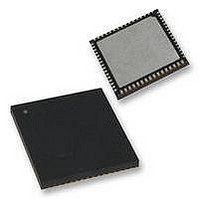
PIC16F1947-E/MR Microchip Technology, PIC16F1947-E/MR Datasheet - Page 350

PIC16F1947-E/MR
Manufacturer Part Number
PIC16F1947-E/MR
Description
28KB Flash, 1KB RAM, 256B EEPROM, LCD, 1.8-5.5V 64 QFN 9x9x0.9mm TUBE
Manufacturer
Microchip Technology
Series
PIC® XLP™ 16Fr
Datasheets
1.PIC16F722-ISS.pdf
(8 pages)
2.PIC16LF1933-ISS.pdf
(46 pages)
3.PIC16LF1946-IPT.pdf
(448 pages)
4.PIC16LF1946-IPT.pdf
(6 pages)
5.PIC16F1946-IPT.pdf
(8 pages)
Specifications of PIC16F1947-E/MR
Core Processor
PIC
Core Size
8-Bit
Speed
32MHz
Connectivity
I²C, LIN, SPI, UART/USART
Peripherals
Brown-out Detect/Reset, LCD, POR, PWM, WDT
Number Of I /o
54
Program Memory Size
28KB (16K x 14)
Program Memory Type
FLASH
Eeprom Size
256 x 8
Ram Size
1K x 8
Voltage - Supply (vcc/vdd)
1.8 V ~ 5.5 V
Data Converters
A/D 17x10b
Oscillator Type
Internal
Operating Temperature
-40°C ~ 125°C
Package / Case
64-VQFN Exposed Pad, 64-HVQFN, 64-SQFN, 64-DHVQFN
Processor Series
PIC16F
Core
PIC
Data Bus Width
8 bit
Data Ram Size
1 KB
Interface Type
MI2C, SPI, EUSART
Maximum Clock Frequency
32 MHz
Number Of Programmable I/os
54
Number Of Timers
5
Operating Supply Voltage
1.8 V to 5.5 V
Maximum Operating Temperature
+ 125 C
Mounting Style
SMD/SMT
3rd Party Development Tools
52715-96, 52716-328, 52717-734
Development Tools By Supplier
PG164130, DV164035, DV244005, DV164005
Minimum Operating Temperature
- 40 C
On-chip Adc
10 bit, 17 Channel
On-chip Dac
5 bit
Lead Free Status / RoHS Status
Lead free / RoHS Compliant
Lead Free Status / RoHS Status
Lead free / RoHS Compliant
- PIC16F722-ISS PDF datasheet
- PIC16LF1933-ISS PDF datasheet #2
- PIC16LF1946-IPT PDF datasheet #3
- PIC16LF1946-IPT PDF datasheet #4
- PIC16F1946-IPT PDF datasheet #5
- Current page: 350 of 448
- Download datasheet (4Mb)
PIC16F/LF1946/47
27.5
The LCD driver module can be configured into one of
four multiplex types:
• Static (only COM0 is used)
• 1/2 multiplex (COM<1:0> are used)
• 1/3 multiplex (COM<2:0> are used)
• 1/4 multiplex (COM<3:0> are used)
The LMUX<1:0> bit setting of the LCDCON register
decides which of the LCD common pins are used (see
Table 27-4
If the pin is a digital I/O, the corresponding TRIS bit
controls the data direction. If the pin is a COM drive,
then the TRIS setting of that pin is overridden.
TABLE 27-4:
27.6
The LCDSEn registers are used to select the pin
function for each segment pin. The selection allows
each pin to operate as either an LCD segment driver or
as one of the pin’s alternate functions. To configure the
pin as a segment pin, the corresponding bits in the
LCDSEn registers must be set to ‘1’.
If the pin is a digital I/O, the corresponding TRIS bit
controls the data direction. Any bit set in the LCDSEn
registers overrides any bit settings in the corresponding
TRIS register.
DS41414B-page 350
Multiplex
Note:
Static
1/2
1/3
1/4
LCD Multiplex Types
Segment Enables
for details).
LMUX
<1:0>
On a Power-on Reset, these pins are
configured as normal I/O, not LCD pins.
00
01
10
11
COMMON PIN USAGE
Unused
Unused
Unused
COM3
Active
Unused
Unused
COM2
Active
Active
Unused
COM1
Active
Active
Active
COM0
Active
Active
Active
Active
Preliminary
27.7
The LCDDATAx registers contain bits which define the
state of each pixel. Each bit defines one unique pixel.
Register 27-6
LCDDATAx registers to the respective common and
segment signals.
Any LCD pixel location not being used for display can
be used as general purpose RAM.
27.8
The rate at which the COM and SEG outputs change is
called the LCD frame frequency.
TABLE 27-5:
TABLE 27-6:
Multiplex
LP<3:0>
Static
Note 1: Clock source is F
1/2
1/3
1/4
2
3
4
5
6
7
2: See
Pixel Control
LCD Frame Frequency
Clock source/(4 x (LCD Prescaler) x 32 x 1))
Clock source/(2 x (LCD Prescaler) x 32 x 2))
Clock source/(1 x (LCD Prescaler) x 32 x 3))
Clock source/(1 x (LCD Prescaler) x 32 x 4))
LFINTOSC.
shows the correlation of each bit in the
Figure
Static
FRAME FREQUENCY
FORMULAS
APPROXIMATE FRAME
FREQUENCY (IN Hz) USING
F
32.768 kHz OR LFINTOSC
122
81
61
49
41
35
OSC
Frame Frequency
2010 Microchip Technology Inc.
27-2.
@ 8 MHz, TIMER1 @
122
1/2
81
61
49
41
35
OSC
/256, T1OSC or
162
108
1/3
81
65
54
47
(2)
=
122
1/4
81
61
49
41
35
Related parts for PIC16F1947-E/MR
Image
Part Number
Description
Manufacturer
Datasheet
Request
R

Part Number:
Description:
IC, 8BIT MCU, PIC16F, 32MHZ, SOIC-18
Manufacturer:
Microchip Technology
Datasheet:

Part Number:
Description:
IC, 8BIT MCU, PIC16F, 32MHZ, SSOP-20
Manufacturer:
Microchip Technology
Datasheet:

Part Number:
Description:
IC, 8BIT MCU, PIC16F, 32MHZ, DIP-18
Manufacturer:
Microchip Technology
Datasheet:

Part Number:
Description:
IC, 8BIT MCU, PIC16F, 32MHZ, QFN-28
Manufacturer:
Microchip Technology
Datasheet:

Part Number:
Description:
IC, 8BIT MCU, PIC16F, 32MHZ, QFN-28
Manufacturer:
Microchip Technology
Datasheet:

Part Number:
Description:
IC, 8BIT MCU, PIC16F, 32MHZ, QFN-28
Manufacturer:
Microchip Technology
Datasheet:

Part Number:
Description:
IC, 8BIT MCU, PIC16F, 32MHZ, SSOP-20
Manufacturer:
Microchip Technology
Datasheet:

Part Number:
Description:
IC, 8BIT MCU, PIC16F, 20MHZ, DIP-40
Manufacturer:
Microchip Technology
Datasheet:

Part Number:
Description:
IC, 8BIT MCU, PIC16F, 32MHZ, QFN-28
Manufacturer:
Microchip Technology
Datasheet:

Part Number:
Description:
IC, 8BIT MCU, PIC16F, 20MHZ, MQFP-44
Manufacturer:
Microchip Technology
Datasheet:

Part Number:
Description:
IC, 8BIT MCU, PIC16F, 20MHZ, QFN-20
Manufacturer:
Microchip Technology
Datasheet:

Part Number:
Description:
IC, 8BIT MCU, PIC16F, 32MHZ, QFN-28
Manufacturer:
Microchip Technology
Datasheet:

Part Number:
Description:
MCU 14KB FLASH 768B RAM 64-TQFP
Manufacturer:
Microchip Technology
Datasheet:

Part Number:
Description:
7 KB Flash, 384 Bytes RAM, 32 MHz Int. Osc, 16 I/0, Enhanced Mid Range Core, Low
Manufacturer:
Microchip Technology

Part Number:
Description:
14KB Flash, 512B RAM, 256B EEPROM, LCD, 1.8-5.5V 40 UQFN 5x5x0.5mm TUBE
Manufacturer:
Microchip Technology
Datasheet:


