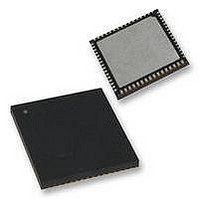
PIC16F1947-E/MR Microchip Technology, PIC16F1947-E/MR Datasheet - Page 58

PIC16F1947-E/MR
Manufacturer Part Number
PIC16F1947-E/MR
Description
28KB Flash, 1KB RAM, 256B EEPROM, LCD, 1.8-5.5V 64 QFN 9x9x0.9mm TUBE
Manufacturer
Microchip Technology
Series
PIC® XLP™ 16Fr
Datasheets
1.PIC16F722-ISS.pdf
(8 pages)
2.PIC16LF1933-ISS.pdf
(46 pages)
3.PIC16LF1946-IPT.pdf
(448 pages)
4.PIC16LF1946-IPT.pdf
(6 pages)
5.PIC16F1946-IPT.pdf
(8 pages)
Specifications of PIC16F1947-E/MR
Core Processor
PIC
Core Size
8-Bit
Speed
32MHz
Connectivity
I²C, LIN, SPI, UART/USART
Peripherals
Brown-out Detect/Reset, LCD, POR, PWM, WDT
Number Of I /o
54
Program Memory Size
28KB (16K x 14)
Program Memory Type
FLASH
Eeprom Size
256 x 8
Ram Size
1K x 8
Voltage - Supply (vcc/vdd)
1.8 V ~ 5.5 V
Data Converters
A/D 17x10b
Oscillator Type
Internal
Operating Temperature
-40°C ~ 125°C
Package / Case
64-VQFN Exposed Pad, 64-HVQFN, 64-SQFN, 64-DHVQFN
Processor Series
PIC16F
Core
PIC
Data Bus Width
8 bit
Data Ram Size
1 KB
Interface Type
MI2C, SPI, EUSART
Maximum Clock Frequency
32 MHz
Number Of Programmable I/os
54
Number Of Timers
5
Operating Supply Voltage
1.8 V to 5.5 V
Maximum Operating Temperature
+ 125 C
Mounting Style
SMD/SMT
3rd Party Development Tools
52715-96, 52716-328, 52717-734
Development Tools By Supplier
PG164130, DV164035, DV244005, DV164005
Minimum Operating Temperature
- 40 C
On-chip Adc
10 bit, 17 Channel
On-chip Dac
5 bit
Lead Free Status / RoHS Status
Lead free / RoHS Compliant
Lead Free Status / RoHS Status
Lead free / RoHS Compliant
- PIC16F722-ISS PDF datasheet
- PIC16LF1933-ISS PDF datasheet #2
- PIC16LF1946-IPT PDF datasheet #3
- PIC16LF1946-IPT PDF datasheet #4
- PIC16F1946-IPT PDF datasheet #5
- Current page: 58 of 448
- Download datasheet (4Mb)
PIC16F/LF1946/47
REGISTER 4-2:
DS41414B-page 58
bit 13
bit 6
Legend:
R = Readable bit
u = Bit is unchanged
‘1’ = Bit is set
bit 13
bit 12
bit 11
bit 10
bit 9
bit 8
bit 7-5
bit 4
bit 2-3
bit 1-0
Note 1:
R/P-1/1
LVP
U-1
2:
—
The LVP bit cannot be programmed to ‘0’ when Programming mode is entered via LVP.
The DEBUG bit in Configuration Word is managed automatically by device development tools including debuggers and
programmers. For normal device operation, this bit should be maintained as a '1'.
LVP: Low-Voltage Programming Enable bit
1 = Low-voltage programming enabled
0 = High-voltage on MCLR/V
DEBUG: In-Circuit Debugger Mode bit
1 = In-Circuit Debugger disabled, RB6/ICSPCLK and RB7/ICSPDAT are general purpose I/O pins
0 = In-Circuit Debugger enabled, RB6/ICSPCLK and RB7/ICSPDAT are dedicated to the debugger
Unimplemented: Read as ‘1’
BORV: Brown-out Reset Voltage Selection bit
1 = Brown-out Reset voltage set to 1.9V
0 = Brown-out Reset voltage set to 2.5V
STVREN: Stack Overflow/Underflow Reset Enable bit
1 = Stack Overflow or Underflow will cause a Reset
0 = Stack Overflow or Underflow will not cause a Reset
PLLEN: PLL Enable bit
1 = 4xPLL enabled
0 = 4xPLL disabled
Unimplemented: Read as ‘1’
VCAPEN>: Voltage Regulator Capacitor Enable bits
0 = V
1 = No capacitor on V
Unimplemented: Read as ‘1’
WRT<1:0>: Flash Memory Self-Write Protection bits
8 kW Flash memory (PIC16F/LF1946 only):
16 kW Flash memory (PIC16F/LF1947):
DEBUG
R/P-1/1
11 = Write protection off
10 = 000h to 1FFh write-protected, 200h to 1FFFh may be modified by EECON control
01 = 000h to FFFh write-protected, 1000h to 1FFFh may be modified by EECON control
00 = 000h to 1FFFh write-protected, no addresses may be modified by EECON control
11 = Write protection off
10 = 000h to 1FFh write-protected, 200h to 3FFFh may be modified by EECON control
01 = 000h to 1FFFh write-protected, 2000h to 3FFFh may be modified by EECON control
00 = 000h to 3FFFh write-protected, no addresses may be modified by EECON control
CONFIGURATION WORD 2
CAP
U-1
—
functionality is enabled on RF0
(2)
W = Writable bit
‘0’ = Bit is cleared
x = Bit is unknown
VCAPEN
CAP
R/P-1/1
U-1
—
pin
PP
must be used for programming
Preliminary
R/P-1/1
(1)
BORV
U-1
—
U = Unimplemented bit, read as ‘0’
-n/n = Value at POR and BOR/Value at all other Resets
P = Programmable bit
STVREN
R/P-1/1
U-1
—
2010 Microchip Technology Inc.
R/P-1/1
R/P-1/1
PLLEN
WRT1
R/P-1/1
WRT0
U-1
—
bit 7
bit 0
Related parts for PIC16F1947-E/MR
Image
Part Number
Description
Manufacturer
Datasheet
Request
R

Part Number:
Description:
IC, 8BIT MCU, PIC16F, 32MHZ, SOIC-18
Manufacturer:
Microchip Technology
Datasheet:

Part Number:
Description:
IC, 8BIT MCU, PIC16F, 32MHZ, SSOP-20
Manufacturer:
Microchip Technology
Datasheet:

Part Number:
Description:
IC, 8BIT MCU, PIC16F, 32MHZ, DIP-18
Manufacturer:
Microchip Technology
Datasheet:

Part Number:
Description:
IC, 8BIT MCU, PIC16F, 32MHZ, QFN-28
Manufacturer:
Microchip Technology
Datasheet:

Part Number:
Description:
IC, 8BIT MCU, PIC16F, 32MHZ, QFN-28
Manufacturer:
Microchip Technology
Datasheet:

Part Number:
Description:
IC, 8BIT MCU, PIC16F, 32MHZ, QFN-28
Manufacturer:
Microchip Technology
Datasheet:

Part Number:
Description:
IC, 8BIT MCU, PIC16F, 32MHZ, SSOP-20
Manufacturer:
Microchip Technology
Datasheet:

Part Number:
Description:
IC, 8BIT MCU, PIC16F, 20MHZ, DIP-40
Manufacturer:
Microchip Technology
Datasheet:

Part Number:
Description:
IC, 8BIT MCU, PIC16F, 32MHZ, QFN-28
Manufacturer:
Microchip Technology
Datasheet:

Part Number:
Description:
IC, 8BIT MCU, PIC16F, 20MHZ, MQFP-44
Manufacturer:
Microchip Technology
Datasheet:

Part Number:
Description:
IC, 8BIT MCU, PIC16F, 20MHZ, QFN-20
Manufacturer:
Microchip Technology
Datasheet:

Part Number:
Description:
IC, 8BIT MCU, PIC16F, 32MHZ, QFN-28
Manufacturer:
Microchip Technology
Datasheet:

Part Number:
Description:
MCU 14KB FLASH 768B RAM 64-TQFP
Manufacturer:
Microchip Technology
Datasheet:

Part Number:
Description:
7 KB Flash, 384 Bytes RAM, 32 MHz Int. Osc, 16 I/0, Enhanced Mid Range Core, Low
Manufacturer:
Microchip Technology

Part Number:
Description:
14KB Flash, 512B RAM, 256B EEPROM, LCD, 1.8-5.5V 40 UQFN 5x5x0.5mm TUBE
Manufacturer:
Microchip Technology
Datasheet:


