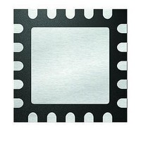
PIC18LF13K22-E/ML Microchip Technology, PIC18LF13K22-E/ML Datasheet - Page 213

PIC18LF13K22-E/ML
Manufacturer Part Number
PIC18LF13K22-E/ML
Description
8KB Flash, 256bytes RAM, 256bytes EEPROM, 16MIPS, NanoWatt XLP 20 QFN 4x4mm TUBE
Manufacturer
Microchip Technology
Series
PIC® XLP™ 18Fr
Datasheets
1.PIC18LF13K22-ISS.pdf
(388 pages)
2.PIC18LF13K22-ISS.pdf
(12 pages)
3.PIC18LF13K22-ISS.pdf
(36 pages)
Specifications of PIC18LF13K22-E/ML
Core Processor
PIC
Core Size
8-Bit
Speed
48MHz
Connectivity
I²C, LIN, SPI, UART/USART
Peripherals
Brown-out Detect/Reset, POR, PWM, WDT
Number Of I /o
17
Program Memory Size
8KB (4K x 16)
Program Memory Type
FLASH
Eeprom Size
256 x 8
Ram Size
256 x 8
Voltage - Supply (vcc/vdd)
1.8 V ~ 3.6 V
Data Converters
A/D 12x10b
Oscillator Type
Internal
Operating Temperature
-40°C ~ 125°C
Package / Case
20-VQFN Exposed Pad, 20-HVQFN, 20-SQFN, 20-DHVQFN
Processor Series
PIC18LF
Core
PIC
Data Bus Width
8 bit
Data Ram Size
256 B
Interface Type
EUSART, I2C, SPI
Maximum Clock Frequency
32 KHz
Number Of Programmable I/os
18
Number Of Timers
4
Operating Supply Voltage
1.8 V to 3.6 V
Maximum Operating Temperature
+ 125 C
Mounting Style
SMD/SMT
3rd Party Development Tools
52715-96, 52716-328, 52717-734, 52712-325, EWPIC18
Development Tools By Supplier
PG164130, DV164035, DV244005, DV164005
Minimum Operating Temperature
- 40 C
On-chip Adc
10 bit, 12 Channel
A/d Bit Size
10 bit
A/d Channels Available
12
Height
0.88 mm
Length
4 mm
Supply Voltage (max)
3.6 V
Supply Voltage (min)
1.8 V, 2.7 V
Width
4 mm
Lead Free Status / RoHS Status
Lead free / RoHS Compliant
Lead Free Status / RoHS Status
Lead free / RoHS Compliant
- Current page: 213 of 388
- Download datasheet (4Mb)
16.2.10
The following registers are used to control the opera-
tion of the ADC.
REGISTER 16-1:
2010 Microchip Technology Inc.
bit 7
Legend:
R = Readable bit
-n = Value at POR
bit 7-6
bit 5-2
bit 1
bit 0
Note 1:
Note:
U-0
—
Selecting reserved channels will yield unpredictable results as unimplemented input channels are left
floating.
ADC REGISTER DEFINITIONS
Analog pin control is performed by the
ANSEL and ANSELH registers. For ANSEL
and ANSELH registers, see Register 8-14
and Register 8-15, respectively.
Unimplemented: Read as ‘0’
CHS<3:0>: Analog Channel Select bits
0000 = AN0
0001 = AN1
0010 = AN2
0011 = AN3
0100 = AN4
0101 = AN5
0110 = AN6
0111 = AN7
1000 = AN8
1001 = AN9
1010 = AN10
1011 = AN11
1100 = Reserved
1101 = Reserved
1110 = DAC
1111 = FVR
GO/DONE: A/D Conversion Status bit
1 = A/D conversion cycle in progress. Setting this bit starts an A/D conversion cycle.
0 = A/D conversion completed/not in progress
ADON: ADC Enable bit
1 = ADC is enabled
0 = ADC is disabled and consumes no operating current
This bit is automatically cleared by hardware when the A/D conversion has completed.
U-0
—
ADCON0: A/D CONTROL REGISTER 0
W = Writable bit
‘1’ = Bit is set
CHS3
R/W-0
CHS2
R/W-0
Preliminary
PIC18F1XK22/LF1XK22
U = Unimplemented bit, read as ‘0’
‘0’ = Bit is cleared
CHS1
R/W-0
CHS0
R/W-0
x = Bit is unknown
GO/DONE
R/W-0
DS41365D-page 213
ADON
R/W-0
bit 0
Related parts for PIC18LF13K22-E/ML
Image
Part Number
Description
Manufacturer
Datasheet
Request
R

Part Number:
Description:
Manufacturer:
Microchip Technology Inc.
Datasheet:

Part Number:
Description:
Manufacturer:
Microchip Technology Inc.
Datasheet:

Part Number:
Description:
Manufacturer:
Microchip Technology Inc.
Datasheet:

Part Number:
Description:
Manufacturer:
Microchip Technology Inc.
Datasheet:

Part Number:
Description:
Manufacturer:
Microchip Technology Inc.
Datasheet:

Part Number:
Description:
Manufacturer:
Microchip Technology Inc.
Datasheet:

Part Number:
Description:
Manufacturer:
Microchip Technology Inc.
Datasheet:

Part Number:
Description:
Manufacturer:
Microchip Technology Inc.
Datasheet:


