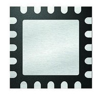
PIC18LF13K22-E/ML Microchip Technology, PIC18LF13K22-E/ML Datasheet - Page 243

PIC18LF13K22-E/ML
Manufacturer Part Number
PIC18LF13K22-E/ML
Description
8KB Flash, 256bytes RAM, 256bytes EEPROM, 16MIPS, NanoWatt XLP 20 QFN 4x4mm TUBE
Manufacturer
Microchip Technology
Series
PIC® XLP™ 18Fr
Datasheets
1.PIC18LF13K22-ISS.pdf
(388 pages)
2.PIC18LF13K22-ISS.pdf
(12 pages)
3.PIC18LF13K22-ISS.pdf
(36 pages)
Specifications of PIC18LF13K22-E/ML
Core Processor
PIC
Core Size
8-Bit
Speed
48MHz
Connectivity
I²C, LIN, SPI, UART/USART
Peripherals
Brown-out Detect/Reset, POR, PWM, WDT
Number Of I /o
17
Program Memory Size
8KB (4K x 16)
Program Memory Type
FLASH
Eeprom Size
256 x 8
Ram Size
256 x 8
Voltage - Supply (vcc/vdd)
1.8 V ~ 3.6 V
Data Converters
A/D 12x10b
Oscillator Type
Internal
Operating Temperature
-40°C ~ 125°C
Package / Case
20-VQFN Exposed Pad, 20-HVQFN, 20-SQFN, 20-DHVQFN
Processor Series
PIC18LF
Core
PIC
Data Bus Width
8 bit
Data Ram Size
256 B
Interface Type
EUSART, I2C, SPI
Maximum Clock Frequency
32 KHz
Number Of Programmable I/os
18
Number Of Timers
4
Operating Supply Voltage
1.8 V to 3.6 V
Maximum Operating Temperature
+ 125 C
Mounting Style
SMD/SMT
3rd Party Development Tools
52715-96, 52716-328, 52717-734, 52712-325, EWPIC18
Development Tools By Supplier
PG164130, DV164035, DV244005, DV164005
Minimum Operating Temperature
- 40 C
On-chip Adc
10 bit, 12 Channel
A/d Bit Size
10 bit
A/d Channels Available
12
Height
0.88 mm
Length
4 mm
Supply Voltage (max)
3.6 V
Supply Voltage (min)
1.8 V, 2.7 V
Width
4 mm
Lead Free Status / RoHS Status
Lead free / RoHS Compliant
Lead Free Status / RoHS Status
Lead free / RoHS Compliant
- Current page: 243 of 388
- Download datasheet (4Mb)
20.0
There are two independent voltage references
available:
• Programmable Voltage Reference
• 1.024V Fixed Voltage Reference
20.1
The voltage reference module provides an internally
generated voltage reference for the comparators and
the DAC module. The following features are available:
• Independent from comparator operation
• Single 32-level voltage ranges
• Output clamped to V
• Ratiometric with V
• 1.024V Fixed Voltage Reference (FVR)
The VREFCON1 register (Register 20-2) controls the
Voltage Reference module shown in Figure 20-1.
EQUATION 20-1:
20.1.3
The comparator voltage reference is V
therefore, the V
V
Voltage Reference can be found in Section 25.0
“Electrical Specifications”.
20.1.4
The V
CV
VREFCON1 register to ‘1’. Selecting the reference volt-
age for output on the V
the digital output buffer and digital input threshold
detector functions of that pin. Reading the CV
when it has been configured for reference voltage out-
put will always return a ‘0’.
Due to the limited current drive capability, a buffer must
be used on the voltage reference output for external
connections to CV
buffering technique.
2010 Microchip Technology Inc.
DD
V
IF D1EN = 1
IF D1EN = 0 & D1LPS = 1 & DAC1R[4:0] = 11111:
IF D1EN = 0 & D1LPS = 1 & DAC1R[4:0] = 00000:
V
V
REF
OUT
. The tested absolute accuracy of the Comparator
OUT
OUT
REF
pin by setting the DAC1OE bit of the
=
VOLTAGE REFERENCES
Voltage Reference
=
=
voltage reference can be output to the device
OUTPUT RATIOMETRIC TO V
VOLTAGE REFERENCE OUTPUT
V
V
V
SOURCE
SOURCE
SOURCE
REF
REF
output changes with fluctuations in
DD
-
+
. Figure 20-2 shows an example
V
+
SS
REF
–
REF
V
SOURCE
pin automatically overrides
OUTPUT VOLTAGE
-
x
--------------------------------
DD
DAC1R[4:0]
derived and
2
5
DD
REF
Preliminary
pin
+
V
SOURCE
PIC18F1XK22/LF1XK22
-
20.1.1
The
comparator configuration. Setting the D1EN bit of the
VREFCON1 register will enable the voltage reference
by allowing current to flow in the V
When the D1EN bit is cleared, current flow in the V
voltage divider is disabled minimizing the power drain
of the voltage reference peripheral.
20.1.2
The
ranges. The 32 levels are set with the DAC1R<4:0>
bits of the VREFCON2 register.
The V
equations:
20.1.5
When the device wakes up from Sleep through an
interrupt or a Watchdog Timer time-out, the contents of
the RECON1 register are not affected. To minimize
current consumption in Sleep mode, the voltage
reference should be disabled.
20.1.6
A device Reset affects the following:
• Voltage reference is disabled
• Fixed voltage reference is disabled
• V
• The DAC1R<4:0> range select bits are cleared
REF
V
voltage
REF
REF
is removed from the CV
output voltage is determined by the following
INDEPENDENT OPERATION
OUTPUT VOLTAGE SELECTION
OPERATION DURING SLEEP
EFFECTS OF A RESET
voltage reference has 32 voltage level
reference
is
REF
independent
REF
DS41365D-page 243
pin
voltage divider.
of
REF
the
Related parts for PIC18LF13K22-E/ML
Image
Part Number
Description
Manufacturer
Datasheet
Request
R

Part Number:
Description:
Manufacturer:
Microchip Technology Inc.
Datasheet:

Part Number:
Description:
Manufacturer:
Microchip Technology Inc.
Datasheet:

Part Number:
Description:
Manufacturer:
Microchip Technology Inc.
Datasheet:

Part Number:
Description:
Manufacturer:
Microchip Technology Inc.
Datasheet:

Part Number:
Description:
Manufacturer:
Microchip Technology Inc.
Datasheet:

Part Number:
Description:
Manufacturer:
Microchip Technology Inc.
Datasheet:

Part Number:
Description:
Manufacturer:
Microchip Technology Inc.
Datasheet:

Part Number:
Description:
Manufacturer:
Microchip Technology Inc.
Datasheet:


