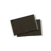
S29JL032H70TFI420 Spansion Inc., S29JL032H70TFI420 Datasheet - Page 12

S29JL032H70TFI420
Manufacturer Part Number
S29JL032H70TFI420
Description
IC,EEPROM,NOR FLASH,2MX16/4MX8,CMOS,TSSOP,48PIN,PLASTIC
Manufacturer
Spansion Inc.
Datasheets
1.S29JL032H70TFI420.pdf
(60 pages)
2.S29JL032H70TFI020.pdf
(64 pages)
3.S29JL032H70TFI420.pdf
(66 pages)
Specifications of S29JL032H70TFI420
Data Bus Width
8 bit, 16 bit
Architecture
Boot Sector
Interface Type
Conventional
Access Time
70 ns
Supply Voltage (max)
3.6 V
Supply Voltage (min)
2.7 V
Maximum Operating Current
2 mA
Mounting Style
SMD/SMT
Memory Type
Flash
Memory Size
32 Mbit
Operating Temperature
+ 85 C
Package / Case
TSOP-48
Lead Free Status / RoHS Status
Lead free / RoHS Compliant
Lead Free Status / RoHS Status
Lead free / RoHS Compliant
Available stocks
Company
Part Number
Manufacturer
Quantity
Price
Company:
Part Number:
S29JL032H70TFI420
Manufacturer:
Spansion
Quantity:
2 356
A D V A N C E
I N F O R M A T I O N
Accelerated Program Operation
The device offers accelerated program operations through the ACC function. This
is one of two functions provided by the WP#/ACC pin. This function is primarily
intended to allow faster manufacturing throughput at the factory.
If the system asserts V
on this pin, the device automatically enters the afore-
HH
mentioned Unlock Bypass mode, temporarily unprotects any protected sectors,
and uses the higher voltage on the pin to reduce the time required for program
operations. The system would use a two-cycle program command sequence as
required by the Unlock Bypass mode. Removing V
from the WP#/ACC pin re-
HH
turns the device to normal operation. Note that V
must not be asserted on
HH
WP#/ACC for operations other than accelerated programming, or device damage
may result. In addition, the WP#/ACC pin must not be left floating or uncon-
nected; inconsistent behavior of the device may result. See “Write Protect
(WP#)” on page 22. for related information.
Autoselect Functions
If the system writes the autoselect command sequence, the device enters the au-
toselect mode. The system can then read autoselect codes from the internal
register (which is separate from the memory array) on DQ15–DQ0. Standard
read cycle timings apply in this mode. Refer to the Autoselect Mode and Autose-
lect Command Sequence sections for more information.
Simultaneous Read/Write Operations with Zero Latency
This device is capable of reading data from one bank of memory while program-
ming or erasing in the other bank of memory. An erase operation may also be
suspended to read from or program to another location within the same bank (ex-
cept the sector being erased).
Figure 21
shows how read and write cycles may be
initiated for simultaneous operation with zero latency. I
and I
in the DC
CC6
CC7
Characteristics table represent the current specifications for read-while-program
and read-while-erase, respectively.
12
S29JL032H
S29JL032HA0 May 21, 2004


