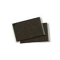
S29JL032H70TFI420 Spansion Inc., S29JL032H70TFI420 Datasheet - Page 33

S29JL032H70TFI420
Manufacturer Part Number
S29JL032H70TFI420
Description
IC,EEPROM,NOR FLASH,2MX16/4MX8,CMOS,TSSOP,48PIN,PLASTIC
Manufacturer
Spansion Inc.
Datasheets
1.S29JL032H70TFI420.pdf
(60 pages)
2.S29JL032H70TFI020.pdf
(64 pages)
3.S29JL032H70TFI420.pdf
(66 pages)
Specifications of S29JL032H70TFI420
Data Bus Width
8 bit, 16 bit
Architecture
Boot Sector
Interface Type
Conventional
Access Time
70 ns
Supply Voltage (max)
3.6 V
Supply Voltage (min)
2.7 V
Maximum Operating Current
2 mA
Mounting Style
SMD/SMT
Memory Type
Flash
Memory Size
32 Mbit
Operating Temperature
+ 85 C
Package / Case
TSOP-48
Lead Free Status / RoHS Status
Lead free / RoHS Compliant
Lead Free Status / RoHS Status
Lead free / RoHS Compliant
Available stocks
Company
Part Number
Manufacturer
Quantity
Price
Company:
Part Number:
S29JL032H70TFI420
Manufacturer:
Spansion
Quantity:
2 356
A D V A N C E
I N F O R M A T I O N
Any commands written to the device during the Embedded Program Algorithm
are ignored. Note that a hardware reset immediately terminates the program
operation. The program command sequence should be reinitiated once that bank
has returned to the read mode, to ensure data integrity. Note that the SecSi Sec-
tor, autoselect, and CFI functions are unavailable when a program operation is in
progress.
Programming is allowed in any sequence and across sector boundaries. A bit
cannot be programmed from “0” back to a “1.” Attempting to do so may
cause that bank to set DQ5 = 1, or cause the DQ7 and DQ6 status bits to indicate
the operation was successful. However, a succeeding read will show that the data
is still “0.” Only erase operations can convert a “0” to a “1.”
Unlock Bypass Command Sequence
The unlock bypass feature allows the system to program bytes or words to a bank
faster than using the standard program command sequence. The unlock bypass
command sequence is initiated by first writing two unlock cycles. This is followed
by a third write cycle containing the unlock bypass command, 20h. That bank
then enters the unlock bypass mode. A two-cycle unlock bypass program com-
mand sequence is all that is required to program in this mode. The first cycle in
this sequence contains the unlock bypass program command, A0h; the second
cycle contains the program address and data. Additional data is programmed in
the same manner. This mode dispenses with the initial two unlock cycles required
in the standard program command sequence, resulting in faster total program-
ming time. Table
13
shows the requirements for the command sequence.
During the unlock bypass mode, only the Unlock Bypass Program and Unlock By-
pass Reset commands are valid. To exit the unlock bypass mode, the system
must issue the two-cycle unlock bypass reset command sequence. (See Table
12).
The device offers accelerated program operations through the WP#/ACC pin.
When the system asserts V
on the WP#/ACC pin, the device automatically en-
HH
ters the Unlock Bypass mode. The system may then write the two-cycle Unlock
Bypass program command sequence. The device uses the higher voltage on the
WP#/ACC pin to accelerate the operation. Note that the WP#/ACC pin must not
be at V
for any operation other than accelerated programming, or device dam-
HH
age may result. In addition, the WP#/ACC pin must not be left floating or
unconnected; inconsistent behavior of the device may result.
4 illustrates the algorithm for the program operation. Refer to the Erase and Pro-
gram Operations table in the AC Characteristics section for parameters, and
Figure 18
for timing diagrams.
May 21, 2004 S29JL032HA0
S29JL032H
33


