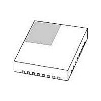
SC16C850VIBS-S NXP Semiconductors, SC16C850VIBS-S Datasheet - Page 27

SC16C850VIBS-S
Manufacturer Part Number
SC16C850VIBS-S
Description
Manufacturer
NXP Semiconductors
Datasheet
1.SC16C850VIBS-S.pdf
(48 pages)
Specifications of SC16C850VIBS-S
Transmitter And Receiver Fifo Counter
Yes
Data Rate
5Mbps
Mounting
Surface Mount
Pin Count
32
Operating Temperature (min)
-40C
Operating Temperature (max)
85C
Operating Temperature Classification
Industrial
Number Of Channels
1
Lead Free Status / RoHS Status
Compliant
NXP Semiconductors
SC16C850V
Product data sheet
7.8 Modem Status Register (MSR)
Table 20.
This register shares the same address as EFCR register. This is a read-only register and
it provides the current state of the control interface signals from the modem, or other
peripheral device to which the SC16C850V is connected. Four bits of this register are
used to indicate the changed information. These bits are set to a logic 1 whenever a
control input from the modem changes state. These bits are set to a logic 0 whenever the
CPU reads this register.
When write, the data will be written to EFCR register.
Table 21.
[1]
Bit
0
Bit
7
6
5
4
3
2
1
0
Whenever any MSR bit 3:0 is set to logic 1, a Modem Status Interrupt will be generated.
Symbol
LSR[0]
MSR[7]
MSR[6]
MSR[5]
MSR[4]
MSR[3]
MSR[2]
MSR[1]
MSR[0]
Symbol
Line Status Register bits description
Modem Status Register bits description
Single UART with 128-byte FIFOs, IrDA, and XScale VLIO bus interface
Description
Receive data ready.
All information provided in this document is subject to legal disclaimers.
Description
CD. During normal operation, this bit is the complement of the CD input.
Reading this bit in the loopback mode produces the state of MCR[3] (OP2).
RI. During normal operation, this bit is the complement of the RI input. Reading
this bit in the loopback mode produces the state of MCR[2] (OP1).
DSR. During normal operation, this bit is the complement of the DSR input.
During the loopback mode, this bit is equivalent to MCR[0] (DTR).
CTS. During normal operation, this bit is the complement of the CTS input.
During the loopback mode, this bit is equivalent to MCR[1] (RTS).
ΔCD
ΔRI
ΔDSR
ΔCTS
logic 0 = no data in Receive Holding Register or FIFO (normal default
condition)
logic 1 = data has been received and is saved in the Receive Holding Register
or FIFO
logic 0 = no CD change (normal default condition)
logic 1 = the CD input to the SC16C850V has changed state since the last
time it was read. A modem Status Interrupt will be generated.
logic 0 = no RI change (normal default condition)
logic 1 = the RI input to the SC16C850V has changed from a logic 0 to a
logic 1. A modem Status Interrupt will be generated.
logic 0 = no DSR change (normal default condition)
logic 1 = the DSR input to the SC16C850V has changed state since the last
time it was read. A modem Status Interrupt will be generated.
logic 0 = no CTS change (normal default condition)
logic 1 = the CTS input to the SC16C850V has changed state since the last
time it was read. A modem Status Interrupt will be generated.
[1]
[1]
Rev. 5 — 19 January 2011
[1]
[1]
…continued
SC16C850V
© NXP B.V. 2011. All rights reserved.
27 of 48


